Tsairus’s Status Reports for 3/28/26

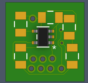
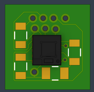
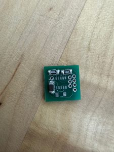
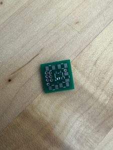
This week I managed to receive the PCB and the components that go with the PCB. After testing, I realized that one of the footprints on the PCB was flipped so the optical flow sensor cannot be solder there else it will destroy the chip. So I will need to most likely reorder the PCB for the final demo and finish the physical testing. Here is the PCB:
I also worked on the code for the integration between the IMU, optical flow sensor, and the MCU so that when the PCB is fully done everything can be easily integrated and tested.

My schedule is behind since I have to reorder the PCB. The actions I will take to catch up is finish fixing the PCB this weekend then reorder it on Monday so that towards the end of the week I can solder it and test it again. Next week I hope to have the PCB fixes done and hopefully have the new PCB received and ready for further testing.
Team Status Report for 3/28/26

The most significant risk right now is that we have to reorder our PCB for our optical sensor. Changes to the PCB are currently being made, and the risk is being managed by shifting our focus towards integrating our parts from the top down rather than bottom up from the sensor. This way, we can ensure our integration flow is working well and the sensor can be easily integrated once our new PCB is in.

No large scale changes have been made to the design of the system, just small scale optimizations and fixes.

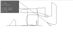
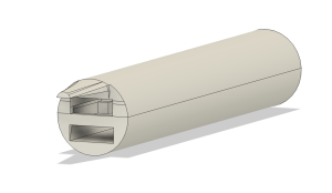
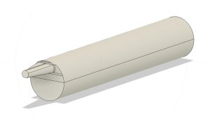
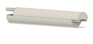
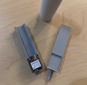
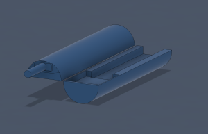
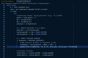
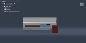
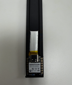
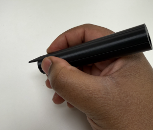
Here is a picture of our current physical stylus with the MCU and battery integrated, and a screenshot of how writing on our canvas currently looks with using dummy data from the IMU rather than optical sensor data.

Christian’s Status Report for 3/28/26

This week I worked on more iterations for our stylus housing, connected our battery to the MCU, and did the first testing of our conversion module with MCU data.

I did a lot more refining of the stylus housing this week to account our PCB wire placement, battery connection, and USB-C wire length. I created more  openings for wires and hollowed out the internals to make more room for the slack that the battery wire connection made.

Since we had some trouble with our sensor PCB, I’m using IMU data from the MCU as dummy dx/dy values, using the BLEHID Adafruit library to feed these values into the OS, and using these values in a largely unchanged conversion module.

My progress is on track, and for next week I hope to help with integrating the optical sensor into our data flow.

Tsairus’s Status Reports for 3/21/26

This week I managed to further test the IMU rotation and tilt for the pen to ensure that it is properly calibrated for the user to comfortably hold the pen. I also spent time thinking through some of the math for how to convert the titled version of the X and Y data from the optical flow sensor into a non-tilted version so that we can properly pass this data to the computer without any discrepancies. Here is the math for that:

Compensated dX = Sensor output dX / Cos(θ)
Compensated dY = Sensor output dY / Cos(Ψ)

My progress is still on track since the PCB and its components should arrive this Monday or Tuesday and I can spend time this week soldering the PCB together. My deliverables for next week is to solder the optical flow sensor PCB together, do some physical testing of the PCB to make sure it is functional, and look more into dynamic CPI adjustment based on how the user tilts the pen to ensure maximum accuracy.

Christian’s Status Report for 3/21/26

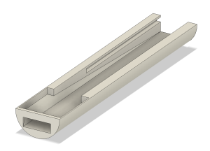
This week I did more refining on our stylus housing. I allocated a bit more room for the internal components since the fit was tight on the last iteration, and I also changed the tip shape to resemble more of a pencil shape. I also added a sliding latch on the back of the pen so that the two halves of the stylus can be held together better, and I extended the length to have a more comfortable hold. My goal right now is to make sure that all components fit well and the writing feels comfortable, then I will reduce the weight of the housing by hollowing out some of the material.

This week I focused more on iterating the housing since we’re still waiting on the optical sensor and pressure sensors to arrive. Both sensors should be in by early next week, so by the interim demo I will have basic functionality of the conversion module with the physical optical sensor and pressure sensor ready. I will take a step back from working on the housing when our sensors and PCB are in, since that is our most major delay.

Team Status Report for 3/21/26

The most significant risk at the moment is the time needed to integrate and test all of our components when our sensor PCB gets in. The rest of our component functionality more or less depends on how well the optical sensor works, and we still need to receive and bring up the PCB. Once this is done though, we should be able to make significantly more progress in the next week and be ready for the interim demo. As stated before our contingency plan is that we have multiple components for our sensor and MCU, and should something not go as planned, we will at least have basic functionality by the interim demo, and time after that to address any issues.

No design changes or schedule updates have been made since last week.

Here are a couple iterations for our stylus housing and MCU fit that we are still iterating.

Christian’s Status Report for 3/14/26

This week I made more edits to our housing design to account for the new size of our sensor PCB, and also experimented with code for integrating a pressure sensor into our design.

The idea behind the revised housing design is for our new sensor PCB to have a good field of view near the tip of the pen, while making the tip a lot narrower so that writing feels more natural.  This thinned out tip design is possible because our new optical sensor is a lot more compact that our initial one. This thinner tip also allows for our sensor to fully utilize its range of angle in the position it’s on our PCB.

I also worked a bit with code that replaces a button click for drawing with a pressure sensor threshold. As mentioned in our team report, we’re aiming to replace some of our button functionality with a pressure sensor, which will eliminate the need for a user to repeatedly press a button to draw versus move.

As mentioned before, progress is just a bit behind because of the waiting period for our sensor, but now that our PCB is getting in next week, I can expedite with lots of testing and tuning next week.

By next week, I will start integrating actual data from our MCU and sensor, since our physical PCB should be getting in by next week.

Team Status Report for 3/14/26

At the moment the most significant risk for our project is correctly integrating all of the parts into our 3D pen case and making sure we mount the optical flow sensor correctly onto the tip of the pen. If any of this is implemented or positioned incorrectly we could lose out on a lot of accuracy with our surface tracking. These risks are being managed by constantly going through different pen case iterations to see which one works the best for our design and overall just doing a lot of testing of the individual components and the components altogether in order to perfect our tuning of the design. The contingency plan we have is plenty of backup components like MCUs and optical flow sensors just in case something breaks and we also left a good amount of time for testing just in case we need to make small design pivots.

The only design changes we’re considering is replacing our initial button integration with a pressure sensor. This allows us to eliminate the need for a user to continually press a button to change between move and draw modes, but rather use pressure thresholds, which feels closer to natural writing. Our schedule remains the same.

Here are some progress pics:


Tsairus’s Status Reports for 3/14/26

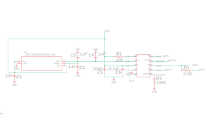
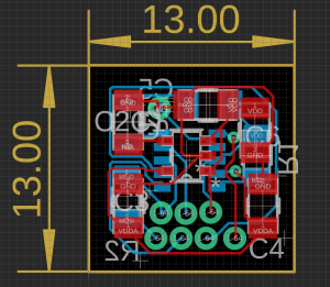
This week I spent time creating the PCB schematics and layout for the optical flow sensor that will help track the pen’s linear movement across any surface. I also spent time looking for the other components that would go on the PCB to support the optical flow sensor like voltage regulators, capacitors, and resistors and put in an order for those. Here are a few images of the schematic, layout, and 3D rendering of what the top and bottom of the PCB will look like:

Top

Bottom

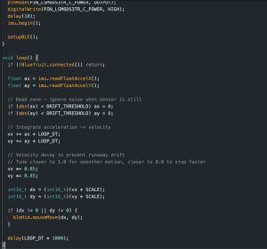
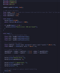
I also spent some time experimenting more with the built in IMU on the XIAO MCU board to test out how we plan on measuring the rotation and orientation of the pen to allow the user to hold the pen in a comfortable way. Here is that test code so far:

My progress is on schedule since I was able to successfully create the PCB and work on some of the IMU implementation. Next week I hope to solder the PCB together and do some physical testing to make sure everything works properly. The PCB should arrive on Monday or Tuesday so I should be able to start soldering it together one of those days.

Christian’s Status Report for 3/7/26

This week I worked more on iterating the 3D housing, as well as planning out testing for when we receive our sensor.

For the 3D housing, I allocated ~1mm of extra space for each component to account for manufacturing differences, and I rearranged the parts so that our MCU can be closer to the tip where users will likely hold the pen, so that our IMU can be more accurate. I also separated out the portion of the housing for the tip so that I can slim out the rest of the body, which will allow for a more comfortable writing experience. I also had to adjust the tip dimensions to account for our new optical sensor.

I haven’t made much progress with the conversion module since I already have the software side of it down as much as I can without having the sensor. Going further with tuning the conversion module has been bottlenecked by our troubles with getting a sensor, so when we actually do have it physically and integrated with our PCB, I can continue in tuning and testing the conversion module for the latency and CPI setting of our physical part. My progress is a bit behind because of this, but since we have our MCU’s in-hand now, I plan to send some “fake” CPI data from the MCU to try and better prime the conversion module for the real data when we get our sensor physically. This, in addition to cutting down in weight on our 3D housing by trimming excess plastic, is what I plan to get done in the next week.