
This week I spent most of the time testing the integration of the IMU and optical flow sensor with the MCU to make sure we were meeting our use case requirements. Most of the testing of those components are done and the main thing that needs to be completed now is tuning the sensitivity of the optical flow sensor and integrating the fsr with everything else. My progress is on schedule and my deliverable for next week is to finish the fsr stuff and finally finishing integrating everything inside the pen.
Team Status Report for 4/18/26
I think the biggest risk we are facing right now is figuring out the best way to integrate the force sensitive resistor (FSR) inside of the pen to allow for easier surface touch and liftoff detection. These risks are being managed by constantly integrating and revisiting the housing design to ensure we get the design for the FSR correct. The contingency plans we have so far is just use a button or two since these are easy to integrate or use the optical flow sensor and IMU together to figure out liftoff detection.
No new changes made to the design and our schedule remains the same.
Tsairus’s Status Reports for 4/18/26
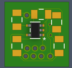
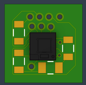
This week I managed to finish assembling the PCB together and doing all the necessary physical testing to make sure the PCB works. I also soldered the wires that we will use to the PCB to make it easier to connect everything to the MCU. When testing the PCB all of the voltages and connections were correct. Here are some pictures of the PCB:
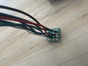
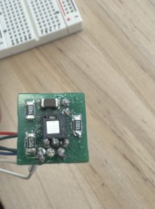
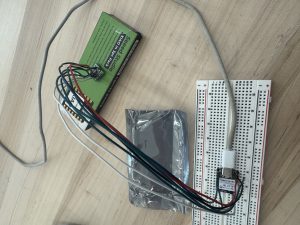
In addition to this, I also wrote some code to test the PCB and MCU integrated together and I was able to successfully get the SPI communication working and the MCU was able to receive the x and y data from the optical flow sensor. One last thing I did was write some test Bluetooth code to see if the PCB and MCU could work together to move my computer mouse by communicating through Bluetooth and this test was successfully as well.
I am currently on schedule and the deliverables I hope to complete next week is integrate the force sensitive resistor with the PCB and MCU to make sure the pressure sensing works and do any last firmware clean up to maximize performance of our system. After that all that is left is just testing.
Week Specific Items
Some knowledge I found necessary to learn in order to accomplishes the task of the project was how IMUs and optical flow sensors worked because without this knowledge I would not have been able to effectively write firmware that could use these components. I also needed to learn more about sensor fusion since our project will be receiving data from different components like an IMU, optical flow sensor, and force sensitive resistor so understanding how to fuse all this data together was important for functionality. In addition to this, I needed to remind myself of good PCB habits since our project needed a very small scale custom PCB and there was not much room for error due to the time constraint. The learning strategies I used to obtain this knowledge is watching a lot of youtube videos and reading a ton of documentation and datasheets. I also used AI from time to time to explain concepts that I was unsure about like how optical flow sensors worked or what does connection interval on Bluetooth mean.
Tsairus’s Status Reports for 4/4/26
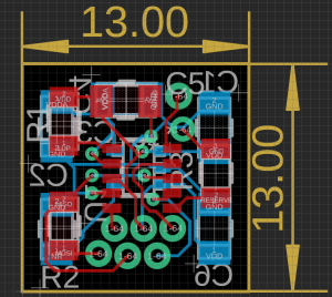
This week I managed to work on the PCB design fixes and submit a new order request for the new updated PCB. Here is the new PCB:
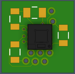
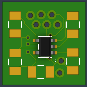
My progress is on schedule and next week I hope to have received the new PCB and solder all of the components onto it. I also want to finish the physical testing of the PCB so that I can focus more on integrating it with the other components.
Week Specific Item
My primary responsibilities are the optical flow PCB, the IMU functionality, and the microcontroller data pipeline. Here are the tests I am thinking about using for verification:
For the optical flow PCB I plan on first doing some physical testing like making sure none of the traces are shorted and all the connections are correct. Then I will run some communication test to ensure the SPI communication is working so I will read the hardcoded product ID of the sensor and make sure the microcontroller receives it correctly. Finally I will run some accuracy test where I will move the PCB 1 inch on a surface and try this with different CPI settings (400, 800, 1200, etc.) and make sure that the sensor outputs the correct number of counts per inch. For example, at 400 CPI when I move the sensor in the x-direction 1 inch the deltaX value should equal around 400.
For the IMU functionality, one test that I already ran is testing how accurate the IMU tilt is so tilting the IMU 0, 30, 45, and 90 degrees and checking what the IMU output was. The IMU tilt was usually within ~3-5 degrees of the tested angle. Another test I was thinking about running was testing how much the IMU drifts using the current smoothing filter we have so if I leave the IMU stationary on a surface for a few minutes I can record how much the IMU angle fluctuates.
For the microcontroller data pipeline, one test I was planning on doing was inputting hardcoded dummy data and eventually real data into the microcontroller and test how well the dynamic CPI function works. For example at a 60 degree tilt and baseline target CPI of 400 the math should be 400/cos(60) which is a new target CPI of 800 so from that I will verify that the microcontroller correctly sends the correct CPI value to the optical flow sensor. I will also run some latency test to make sure all if this processing happens under the time constraint.
Tsairus’s Status Reports for 3/28/26
This week I managed to receive the PCB and the components that go with the PCB. After testing, I realized that one of the footprints on the PCB was flipped so the optical flow sensor cannot be solder there else it will destroy the chip. So I will need to most likely reorder the PCB for the final demo and finish the physical testing. Here is the PCB:
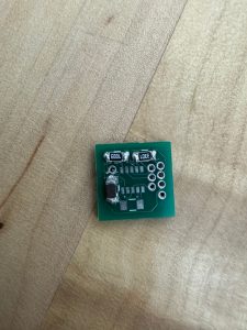
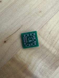
I also worked on the code for the integration between the IMU, optical flow sensor, and the MCU so that when the PCB is fully done everything can be easily integrated and tested.
My schedule is behind since I have to reorder the PCB. The actions I will take to catch up is finish fixing the PCB this weekend then reorder it on Monday so that towards the end of the week I can solder it and test it again. Next week I hope to have the PCB fixes done and hopefully have the new PCB received and ready for further testing.
Tsairus’s Status Reports for 3/21/26
This week I managed to further test the IMU rotation and tilt for the pen to ensure that it is properly calibrated for the user to comfortably hold the pen. I also spent time thinking through some of the math for how to convert the titled version of the X and Y data from the optical flow sensor into a non-tilted version so that we can properly pass this data to the computer without any discrepancies. Here is the math for that:
Compensated dX = Sensor output dX / Cos(θ)
Compensated dY = Sensor output dY / Cos(Ψ)
My progress is still on track since the PCB and its components should arrive this Monday or Tuesday and I can spend time this week soldering the PCB together. My deliverables for next week is to solder the optical flow sensor PCB together, do some physical testing of the PCB to make sure it is functional, and look more into dynamic CPI adjustment based on how the user tilts the pen to ensure maximum accuracy.
Team Status Report for 3/14/26
At the moment the most significant risk for our project is correctly integrating all of the parts into our 3D pen case and making sure we mount the optical flow sensor correctly onto the tip of the pen. If any of this is implemented or positioned incorrectly we could lose out on a lot of accuracy with our surface tracking. These risks are being managed by constantly going through different pen case iterations to see which one works the best for our design and overall just doing a lot of testing of the individual components and the components altogether in order to perfect our tuning of the design. The contingency plan we have is plenty of backup components like MCUs and optical flow sensors just in case something breaks and we also left a good amount of time for testing just in case we need to make small design pivots.
The only design changes we’re considering is replacing our initial button integration with a pressure sensor. This allows us to eliminate the need for a user to continually press a button to change between move and draw modes, but rather use pressure thresholds, which feels closer to natural writing. Our schedule remains the same.
Here are some progress pics:
Tsairus’s Status Reports for 3/14/26
This week I spent time creating the PCB schematics and layout for the optical flow sensor that will help track the pen’s linear movement across any surface. I also spent time looking for the other components that would go on the PCB to support the optical flow sensor like voltage regulators, capacitors, and resistors and put in an order for those. Here are a few images of the schematic, layout, and 3D rendering of what the top and bottom of the PCB will look like:
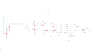
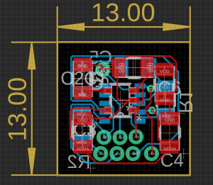
Top
Bottom
I also spent some time experimenting more with the built in IMU on the XIAO MCU board to test out how we plan on measuring the rotation and orientation of the pen to allow the user to hold the pen in a comfortable way. Here is that test code so far:
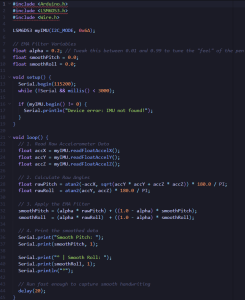
My progress is on schedule since I was able to successfully create the PCB and work on some of the IMU implementation. Next week I hope to solder the PCB together and do some physical testing to make sure everything works properly. The PCB should arrive on Monday or Tuesday so I should be able to start soldering it together one of those days.
Team Status Report for 3/7/26
Previously our most significant risk was actually getting the motion sensor but after working with the vendor we finally received the sensor and datasheet that we wanted and now need to make a PCB for it. So we think now the biggest risk is just receiving the PCB on time before our interim demo and making sure we have the 3D printed casing ready for all of our parts. The PCB will be completed by this weekend so it can be sent of Monday which ideally should be enough time to receive it before the demo and the 3D case has been going through multiple iterations as well to ensure all the components fit. The main contingency plan we have is if the PCB does not arrive in time we do have another backup motion sensor that we took from a mouse that is a through hole component so we could temporally wire it up to a breadboard or something just to show our design working until we receive the PCB.
There has been one change to our design which is the type of optical flow sensor. We have managed to receive an optical flow sensor with a different part number and is much smaller than the previous one we were considering. This change was necessary since the other optical flow sensors we hard to find and this was the one the vendor recommended to us. In addition, the other optical flow sensors are much bigger so with this new one would allow our pen tip to be smaller. We think the only cost we incur from this change is we will most likely need to change our pen tip size to fit the new motion sensor other than that everything else pretty much remains the same. We will just continue to experiment with the 3D pen case to mitigate this.
Here is our updated schedule: 18-500 Gantt chart – Gantt Chart
Week-Specific Items
A was written by T’sairus Beasley, B was written by Christian Cherry, and C was written by Jamari Toussaint.
Part A (Global Factors): To address global factors, our digital pen is designed to break down the geographic and socioeconomic barriers associated with digital education and creative work. In many regions and non-academic environments, users lack access to expensive hardware like tablets or specialized displays. By utilizing an optical flow sensor and IMU inside of a pen to track movement on any standard surface like a basic wooden desk our product allows anyone with a basic, low-cost Bluetooth-enabled laptop to have access to high-quality digital tool. Furthermore, the pen’s architecture directly accommodates users who are not technologically savvy since the onboard MCU handles all the complex coordinate transformation math locally and the pen acts as an universal Bluetooth device. This means users around the world are not required to download specialized drivers, navigate complex software installations, or pay for subscription ecosystems. Our device makes digital literacy and tools globally accessible.
Part B (Cultural Factors): The transition from physical to digital mediums can often disrupt traditional methods of writing and artistic expression. To address these cultural factors, our stylus respects these by very closely mimicking the physical form factor, weight, and tactile experience of a traditional pen. In addition to this, by calculating orientation with the IMU and MCU locally and transmitting these results to the digital canvas, our stylus preserves the user’s natural handwriting style and stroke dynamics. This ensures that users are not forced to adapt their cultural writing behaviors to suit rigid technology. Instead our stylus technology seamlessly adapts to the physical habits of the user and allows their experience to feel more natural and align with the norm.
Part C (Environmental Factors): To address environmental factors, our design mitigates the issues typically associated with traditional writing. Traditional writing consumes tons of paper and contributes to negative environmental impacts such as deforestation. Our pen design eliminates the need for paper entirely and allows users to digitize their work by writing directly on any desk or table surface which are inherently reusable surfaces. Also the pen implementation reduces electronic waste by integrating a rechargeable LiPo battery and utilizing lead-free solder on the custom PCB. This helps the pen avoid the toxic metal waste generated by disposable alkaline batteries. Finally, the modular design of the pen case allow users to open the casing and replace individual components rather than discarding the entire pen if a single part fails.
Tsairus’s Status Reports for 3/7/26
This week I spent time working on fleshing out the optical subsystem and power subsystem for the design report. I also spent some time analyzing the tradeoffs between our design choices and portraying those in tables to help better show how our design came about. For the optical subsystem, I spent time deriving the equations for how we calculated the CPI that will be used by our pen and I finalized which optical flow sensor we will be using for our design. Here is the CPI calculation for our pen:

For the power subsystem, I spent time deriving the equations for what our power system will look like and why we chose the battery we are going with. Here is the calculations for that:

One last thing I did this week outside of the design report stuff is I spent time working with the vender of the optical flow sensor to receive the proper optical flow sensor and datasheet that we want to use for our pen. The optical flow sensor has been received and now the biggest thing to work on is the PCB for it.
My progress is a little behind because I was hoping to have the PCB done and sent off before spring break but I was waiting for the vendor to approve of me receiving the datasheet and the sensor. This minor setback should be okay since I plan on finishing the PCB today and tomorrow so it can be sent off to the fab on Monday. So my main deliverables for this week is to finish the optical flow sensor PCB this weekend and spend next week setting up our microcontroller and working on the IMU implementation for the orientation of the pen while we wait to receive the PCB.