Team Status Report 3/18

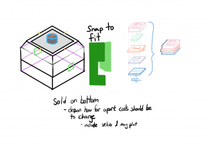
Currently the risks are the same from last week, but much more mitigated now. We have a 3D design of the housing and can confirm the dimensions in the following week when we have fully assembled keys to see how much room we can have and shave down. Currently the dimensions are 25x25x23 mm^3 (w x l x h), and this is with most likely more leeway than is needed. Since it appears we can have 3D housing finished soon, that worry is one less. The programming software unfortunately cannot be started until we have working prototype of the whole system set up, however with the progress of the receiver and BLE boards, we should be reaching that goal soon.

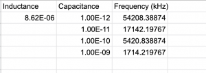
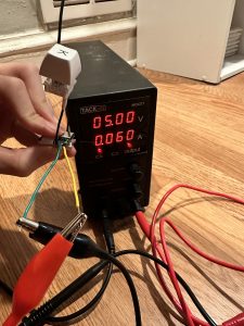
The wireless charging kits came this week so that we may begin working on the proof of concept next week as well. This will be helpful in determining on how fast the charging will be once we have made our adjustments.

No significant changes have been made since last update.

Our schedule is on track as we were able to do 3D housing this week.

New tools: Using Solid Works instead of Autodesk due to more familiarity and no need to import the BLE footprint. Solder iron to solder the keys together with the hot swap boards.

Currently with 4 keys connecting to one another, the receiver acting as a keyboard, 2 key modules assembled, and solid works file of the 3D housing(forgot to take screenshot), we have made good progress.

Korene’s Status Report 3/18

This week completed ethics assignment and the 3D housing design in solid works. Unfortunately, this proof does not have screenshots because I had forgotten to take them, but the files are in Box.

It was necessary to spend a while on refreshing solid works knowledge and relearning some shortcuts. I used these tutorials for guidance on snap fit joints and splitting parts

Completing the 3D housing base was relatively simple overall, however, I followed the tutorials above to ensure it would be a smoother process. Still in the progress of making the joints as there are some issues with the joint sketch and extrusion of it. Printing out the joints will also be a different thing as we will have to edit the spacing a few times to ensure a smooth fit.

We also received the inductive charging kit so next week I plan to get a prototype of inductive charging with Zhejia next week as well.

Currently this is good progress made, not stuck on thinking about what parts to buy and we can continue working towards the goal.

Zhejia’s Status Report 3/18

This week I worked on creating a prototype for the keyboard firmware that acts as an interface between the key receiver and the computer. I prototyped this on the Arduino Nano 33 IoT, since the Arduino Keyboard library was not compatible with the Seeed Xiao boards. However, this caused a few issues since to get the keyboard working, a new driver was needed for the Nano 33 IoT. Additionally, I had to make sure the right version of the Keyboard and USB libraries were installed, as there were some issues posted online with the keyboard device not being recognized in certain versions. Finally, I modified the KeyReceiver code to be able to distinguish between the individual key presses and send a different character as a keyboard depending on which key was pressed.

I am on schedule this week since I was scheduled to work on the keyboard programming software, and having the Arduino being able to act as a keyboard was an important first step to this.

Next week, I hope to finish the code template that the keyboard customization software will edit and flash to the main board.

Ben’s Status Report 3/18

This week I worked on implementing multiple connections with the central receiver. I managed to get 4 keys working since we only had 4 batteries in total. I also figured out the layout of the battery, switch, and board. Originally, we planned to have the battery sandwiched between the two boards (the Seeed and the single switch PCB). However, after some consideration, I determined it would be too difficult to solder consistently while keeping everything in place. Thus, I modified the design to have the Seeed flipped with the single switch PCB stacked on the back of the board and the battery on the front. This allowed easier access to the reset switch and protected the battery connection. Using this design, I soldered together 2 boards. I also soldered the Mill Max sockets onto the PCBs, which allowed hot-swapping of the switches. On the software side, I managed to get interrupt based signaling working. This means that the peripherals will only attempt to send data over if a key is pressed, and sleep otherwise, thus saving power. Additionally, I set the rest of the pins on the board to be input pullup to reduce power draw further. Finally, on the receiver side, I managed to get reconnection working. However, this reconnection is very slow, taking up to 30 seconds in some cases. To test sizing and consistency. Overall, this design ended up with a thickness of 15mm, which gives us 7mm of space for the wireless charging module.

I believe my progress is on schedule, since this week I was slated to work on the connection of multiple switches and the housing. I have the rough dimensions of the housing finalized thanks to finally having the height of entire assembly set, and I have also managed to connect 4 separate boards to the central receiver. Next week I hope to assemble more boards and reduce the latency of reconnection and optimize the interrupts more. Currently the interrupts occasionally lock up the board, requiring a reset. I hope to figure out how to resolve this issue next week as well.

Korene Tu’s Status Report 3/11

We’ve decided to buy some new products for wireless charging and in terms of the project we’ll be figuring out the protocols of connecting the keys to the MCU to the computer, in which case more embedded programming is necessary to learn how to clarify and how that works in practice.


Majority of the week was spent on the design review reports and organizing the plan of what we had up until now. Through writing the design review, I figured out where we were in our budget which may be a concern but can now be warier of how to spend our budget. In addition, writing out the whole plan thus far helps to figure out where any more vague plans were vs. what we can easily explain was well thought out.

Afterward, I drafted a drawn plan of the 3D housing for the keys and saw what interlocking method we would use(snap-to-fit cantilever joints), and estimated the size. Overall, in order to have a snug fit we’ll probably have about 5% more room than needed from a tight fit to be looser.

I made a quick table of what capacitors would be needed to have what frequency for the inductor coils which are.


Overall some difficulties are figuring out the microcontroller next and waiting for some parts. Maybe some time crunch but now that we’re over the first half of buying items we can continue onwards.

Team Status Report 3/11

Currently, we believe the most significant risks are that the wireless charging may not be able to deliver enough current to charge the battery sufficiently quickly and that the timeline may not allow for sufficient time to iterate both the programming software and the design of the 3D printed housing by the time the project is due. In terms of wireless charging, we are managing the risk by focusing development on getting a single switch to wireless charge correctly as a proof of concept, and having the remaining switches charge from USB as a backup. In terms of the software, we plan to focus on functionality first and then add any aesthetic improvements only if we have time. The same goes for the 3D printed housing. We may have to end up sacrificing some of the dimension design requirements to get the housing working at first, but then we plan to see what we can shave down after the fact.

We added a single switch PCB as an interface between the Cherry MX switch and the Seeed board. This was necessary as we found that our original plan of soldering wires between the switches and Seeed board would not meet the requirement of having hotswap capabilities. Additionally, it would make assembly nearly impossible as the switch would have to somehow be soldered inside the housing. This incurs an additional $1.50 cost per switch, but since the PCBs are so simple, it would cost a lot less if we ordered custom PCBs (~$5 on JLPCB). However, since we want to begin putting everything together more quickly, Amazon seemed to be the better choice. With this change, we may need to increase the dimensions of the housing to occupy a footprint of 25mmx22mm as current measurements of the battery + seeed setup already are pushing 22mm in the length dimension. We believe that this will not present that large of a usability issue however, since that is about the difference in spacing between a laptop keyboard and a Cherry MX style keyboard, and thus we do not expect users to be able to notice a difference.

There are no updates to the schedule currently. We have attached images of our charging testing and a video of the two switch connection working.

New tools:

To design the software, we would need to learn some sort of GUI creation library like PyGUI or GTK. To design the 3D printed housing, we plan on learning how to design using Autodesk, since it allows us to import Eagle footprints in order to give us an idea of the dimensions of the Seeed board and other components.

Video link: https://youtu.be/-SggOrEHb1I

Zhejia’s Status Report 3/11

This week, I worked on the interface between the magnetic charging and the seeed xiao BLE board. I researched the schematic diagrams and tested which pins can be used to charge the LIPO battery through the seeed board. We don’t want to directly charge the LIPO since the seeed board has a battery management system (BMS) already (BQ25100) which guarantees safe charging since overcharging LIPO batteries is dangerous. Looking through this schematic diagram, which is for the sense version of the board, but is the same ignoring the sense components, I found that charging is done though V_BUS, which is connected to the BMS, so the next step was trying to find an external pin that connected to V_BUS.  The pinout sheet given on the official website had it labeled as AD2 instead, so I spent some time trying to find which external pin was AD2 to no avail. Later, after examining the schematic again, I realized that this pinout sheet was for the nrf52840 chip instead of the seeed board. Although none of the pinout diagrams for the board officially labelled a pin as V_BUS, I presumed V_USB was likely connected to V_BUS since the USB was connected to V_BUS in the schematic. Then I used my power supply to provide 5V to the V_USB pin (pictures on the team status report), and at first it did not work, so I thought that V_USB might be connected to V_IN instead of V_USB, which would be an issue, but actually, the issue was connecting the ground pin to the ground terminal of the power supply did not work and it instead needed to be connected to the negative terminal of the power supply. In the end, I successfully charged the LIPO with 3.25V-5.5V although the 3.25V only provided 8mA of current while it basically gets full current of 60mA at 4.35V which matches the recommended operating conditions of V_USB in the datasheet. According to the datasheet, we also should be able to charge with low voltages using the VDD pin, but I have not tested that.

Of course, I worked on the design report as well.

My progress is on schedule, and I plan to research and start writing the keyboard driver software to send keypress data to the computer next week.

Ben’s Status Report 3/11

This week I worked on implementing the connection between multiple Seeed BLE boards and a central controller. To facilitate this, I modified the peripheral code, having each Seeed board’s characteristic utilize the notify function to allow the central board to subscribe to multiple peripherals at once. Unfortunately, because I only brought 2 Seeed boards home, I had to buy a Arduino Nano 33 IoT to test the multi board connection. Luckily, the BLE library worked fine with the board and I was able to test the central connecting with two peripherals simultaneously. The code has been updated on the github to reflect these changes. I also wrote the Introduction, Use-Case requirements, Architecture, and Design Requirements sections of the design report and helped with the Design studies, Summary, and Glossary of Terms.

This work puts me a bit ahead of schedule since I believe this will allow me to scale up to multiple switch devices without much hassle.

Next week I plan to get multiple keys working and, when the single switch PCBs get here, solder together the switch breakout board with the Seeed boards and test their stability.

Here is a video of the two key receiver working: https://youtu.be/-SggOrEHb1I

Korene’s Status Report 2/25


This week was a lot of research into what components to buy. We had the proof of concept from last week but realized finding other components would prove to be a bit more difficult than expected. The first thing was the needed addition of a sine wave oscillator, we thought of a few options: using a Colpitts oscillator, a 555 timer with capacitors to make the sine wave, a VCO, or buying a whole wireless charging IC that would have it’s own pair of receiver and transmitter IC chips to then use and adjust. The problem with a Colpitts oscillator would be the math may not be as accurate, same thing with the 555 timer as it may prove to have slightly off frequency wave generation. In addition, we’ll need a power amplifier to increase the voltage and current output of the wave generated. Finding a good VCO on Digikey was oddly difficult, either needed to buy 50 in bulk or it was still a square wave generator or it ended up being a microcontroller itself. In addition, we’ll need to have something that can generate a specific voltage for that. Zhejia and I have spent most of Saturday and Wednesday searching for different ICs that could fulfill our needs. Most appeared to be much more complex than we needed and take up too much space. We found one that appears to be great for our usage in terms of size and simplicity and is also used quite often in other wireless charging products– XKT-510 for the transmitter and T3168 for the receiver as a pair from Taidacent or P9235 and P9222 from Renesas.

We’re a bit behind due to the unknown factors seen in buying the PCB parts, hopefully by Monday we can decide on a product to run with, and from there we’ll start the PCB schematics.

Weekly Question: enumerate how you have adjusted your teamwork assignments to fill in gaps related to either new design challenges or team shortfalls (e.g. a team member missing a deadline)

Zhejia and I have doubled down on the search to ensure we can figure out what parts we really need. Ben has stayed on track pretty consistently so I’ve mainly been focused on my tasks to come to a decision on parts to resolve the issue.

We shall enter the purchase form next week and I look to have a pcb schematic of parts, perhaps even start on layout and looking into what is needed to fulfill requirements.

Team Status Report – 2/25

Risks:

The turnaround time for PCBs added with the shipping time of the XKT ICs and testing the PCB is cutting off much of our margin for error allowance and is dangerously late. 3 weeks for PCB turnaround, 1 week for IC chip shipping, and 1 week for PCB testing goes for a total of 5 weeks, which would not leave us enough time to remake the PCB if anything goes wrong.

To manage this, we will make the PCB layout next week without specific values for the capacitors to have the PCB design basically ready except for specific values. Additionally, we will test the circuit on a breadboard before sending the PCBs out to fabricate, and ideally, we can choose a fabrication lab that will have a faster than 3-week turnaround.

Another risk is the latency of the BLE communication, since BLE only allows one server to be connect to one client at a time, and there is a minimum connection time of ~7ms required. Our current mitigation strategy is to daisy-chain multiple keys together so each seeed BLE board can connect as a client to one other board and also connect as a server to a different board. Aka the boards can for a chain of board1 -> board2 -> board3 -> board4 -> … -> Main board and board9-> board10 -> etc to minimize the connection switching necessary.  The number of chains that would give the fastest connection is still to be determined next week.

Changes:

No changes were made to the design of the system since last week.

Schedule updates:

Since the IC and PCB will take at least a week to ship and our design was delayed due to having issues figuring out the wireless charging system, we have shifted later tasks such as writing/designing the configurator software up.

Team Work Adjustments:

The new design challenge of delivering enough current through the wireless inductive charging transmitter resulted in a week of much research and comparing pros and cons to creating the circuit ourselves and what types of chips we could feasibly get and use, and has pushed around our schedule such that we will have to push back integration of our entire wireless charging system to when the IC chips and coils arrive. Additionally, the PCB send out for fabrication was also delayed by this week and the IC chip shipping week, so in order to maximally use the weeks of waiting, we have adjusted our work assignments to preparing for when components arrive and focusing on other parts of our project that don’t require those components.