Korene’s Status Report 4/22

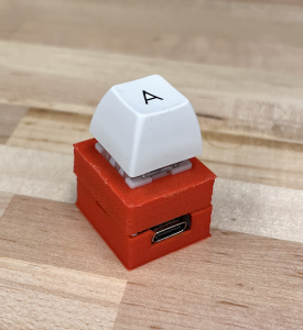
This week did testing and final iterations of key housing.
We finished up tests of the project for latency, inductive charging speed, battery life of keys, portability, and stability. This concludes the final data needed in our report and final presentation slides. We all met up to conclude the tests and I made the necessary calculations in budget to sum-up the purchases of what we’ve made so far. More calculations done to figure out an estimate of our power capabilities done as well. The iPhone slow motion camera was efficient enough to capture the latency, so it wasn’t a problem whatsoever.

Fit wise, the housing is successful but need thicker walls to keep the housing stable. In addition have realized I’ve been using the wrong settings for slicing the print because I’ve been setting the 3D printer to the wrong one in using Cura, which may be a factor into some bugs in printing. Final print will be done Sunday and shall be finishing up the presentation slides. Integration as a whole has been alright, the things left are extra items to make the whole package look nicer in general. Housing being done means we can solidify our weight count for the whole product, as of now it is 371 grams including the previous iteration of 3D housing

We are on track to finishing the projecting and doing my part in contribution.

Ben’s Status Report 3/18

This week I worked on implementing multiple connections with the central receiver. I managed to get 4 keys working since we only had 4 batteries in total. I also figured out the layout of the battery, switch, and board. Originally, we planned to have the battery sandwiched between the two boards (the Seeed and the single switch PCB). However, after some consideration, I determined it would be too difficult to solder consistently while keeping everything in place. Thus, I modified the design to have the Seeed flipped with the single switch PCB stacked on the back of the board and the battery on the front. This allowed easier access to the reset switch and protected the battery connection. Using this design, I soldered together 2 boards. I also soldered the Mill Max sockets onto the PCBs, which allowed hot-swapping of the switches. On the software side, I managed to get interrupt based signaling working. This means that the peripherals will only attempt to send data over if a key is pressed, and sleep otherwise, thus saving power. Additionally, I set the rest of the pins on the board to be input pullup to reduce power draw further. Finally, on the receiver side, I managed to get reconnection working. However, this reconnection is very slow, taking up to 30 seconds in some cases. To test sizing and consistency. Overall, this design ended up with a thickness of 15mm, which gives us 7mm of space for the wireless charging module.

I believe my progress is on schedule, since this week I was slated to work on the connection of multiple switches and the housing. I have the rough dimensions of the housing finalized thanks to finally having the height of entire assembly set, and I have also managed to connect 4 separate boards to the central receiver. Next week I hope to assemble more boards and reduce the latency of reconnection and optimize the interrupts more. Currently the interrupts occasionally lock up the board, requiring a reset. I hope to figure out how to resolve this issue next week as well.

Team Status Report – 2/25

Risks:

The turnaround time for PCBs added with the shipping time of the XKT ICs and testing the PCB is cutting off much of our margin for error allowance and is dangerously late. 3 weeks for PCB turnaround, 1 week for IC chip shipping, and 1 week for PCB testing goes for a total of 5 weeks, which would not leave us enough time to remake the PCB if anything goes wrong.

To manage this, we will make the PCB layout next week without specific values for the capacitors to have the PCB design basically ready except for specific values. Additionally, we will test the circuit on a breadboard before sending the PCBs out to fabricate, and ideally, we can choose a fabrication lab that will have a faster than 3-week turnaround.

Another risk is the latency of the BLE communication, since BLE only allows one server to be connect to one client at a time, and there is a minimum connection time of ~7ms required. Our current mitigation strategy is to daisy-chain multiple keys together so each seeed BLE board can connect as a client to one other board and also connect as a server to a different board. Aka the boards can for a chain of board1 -> board2 -> board3 -> board4 -> … -> Main board and board9-> board10 -> etc to minimize the connection switching necessary.  The number of chains that would give the fastest connection is still to be determined next week.

Changes:

No changes were made to the design of the system since last week.

Schedule updates:

Since the IC and PCB will take at least a week to ship and our design was delayed due to having issues figuring out the wireless charging system, we have shifted later tasks such as writing/designing the configurator software up.

Team Work Adjustments:

The new design challenge of delivering enough current through the wireless inductive charging transmitter resulted in a week of much research and comparing pros and cons to creating the circuit ourselves and what types of chips we could feasibly get and use, and has pushed around our schedule such that we will have to push back integration of our entire wireless charging system to when the IC chips and coils arrive. Additionally, the PCB send out for fabrication was also delayed by this week and the IC chip shipping week, so in order to maximally use the weeks of waiting, we have adjusted our work assignments to preparing for when components arrive and focusing on other parts of our project that don’t require those components.

Weekly Status Report 2/18

We believe the most significant risks currently involve getting the custom PCBs in on time and getting the wireless charging current high enough. We would like to have a 50mA charging current minimum, which would hopefully reach our target of under 8 hours charging time with buffer to spare. However, our current charging capabilities of < 1mA would mean that charging the battery to full would take astronomically long. Like last week, our backup plan if the PCBs do not get here on time, is to use one of the SEEEDs as a central receiver. For the charger, our backup plan is to use the USB port attached to a wireless charging pad.

There were some changes to the wireless charging setup, which are documented in Zhejia’s individual status report. This change was necessary to reach the minimum charging voltage on the SEEED. This does not incur many additional costs, as we still need to design the custom PCBs.

Our schedule remains unchanged.

Wireless working:

https://youtube.com/shorts/qfVXAoujZhY?feature=share