4/29 Korene’s Status Report

This week finalized on key housing design and now in process of printing 16 housings, I flipped the fastening joints to the bottom part of the housing for a better fit, and now the finalized sizing is 24mm x 23mm x 20mm (LxWxH) which fits our sizing constraints better. Overall went through 4 iterations of housing design and fittings. Overall process was a bit slower due to access to 3D printer mishaps

Will be well prepared for next week’s demo, just need to attach velcro on the housings. For inductive coiling, we’ll be waiting on a plug in order to connect to a wall outlet. Overall not much testing to be done here, keys do not wobble at all on their own even now so with velcro they should be quite stuck

Korene’s Status Report 4/8

This week Question:

  1. Now that you are entering into the verification and validation phase of your project, provide a comprehensive update on what tests you have you run or are planning to run. In particular, how will you analyze the anticipated measured results to verify your contribution to the project meets the engineering design requirements or the use case requirements?
    Inductive coil testing: We’ve been making tests at the outputs of the transmitter coil to see what wave is outputted and what is the output voltage by using an oscilloscope to measure at the two inductor points. This allows us to know if the period is what we expect, if the peak to peak voltage is not being shorted or other reasons it may be lower than anticipated and if our output is still a sine like wave. This is primarily for debugging currently, but later on this will be useful to measure what our power efficiency is when we also measure how much current there is going through as well.
    With power efficiency, we’ll also be testing the duration of how long it takes to charge and this will also be related to the power transfer. One method is through using a stop watch and timing how long it takes to charge fully one (as of now it seems to be relatively quickly through a USB-C, so we may be able to measure the whole battery journey from start to finish). It’s important to measure the entire battery charge as it is a curved relation and not linearly, as it becomes more full, it becomes slower to charge.

    For 3D housing, that is just using calipers to measure. We can see how large it is and then also take into account in usage of whether it is comfortable to type on. Perhaps as an addition to the case we will include a wrist rest as the package of components is quite tall, however this is also a normal occurence in high end keyboards. Stability wise has not appear to be an issue either, but we will take into account of a wobble factor (perhaps measured by multiple people seeing how much effort it takes to knock a key down?)
    This week Progress
    This week I made another iteration of changes to the 3D housing and testing for the inductive coiling to determine what configuration the circuit is in. 

Inductive coil: Issues this week were unfortunately soldering issues to create a good pin output to the breadboard with the inductive coils. A few of the solder pads were ripped off due to uncareful measures, but that is just technical difficulties. That’s caused some slow down with circuit testing

We were able to measure the output of the oscillator chip directly (XKT-412) which we determined is similar to a 555 Timer due to it’s constant output. This denotes that our issues with inductive charging is with the power amplifier. Because of the larger resistance of the smaller coils, it affects how the power is transferred. We are still looking through some literacy to understand what could be helped with this, I’ve been referencing some of my 18-421 notes about common source amplifiers to see what the specific remedy could be and if it is just the common source amplifier or if it could have multiple power amplification stages.

3D Housing: After multiple runs through faulty 3D printing machines and a good print, I’ve determined the walls were made much too thin. I’ve thickened the walls to go from 1mm to 1.25mm and the back wall (which was thinner to account for a longer piece) to be at least 1mm now.

Printing a 1mm wall works fine, but a .6mm wall did not print anything out. Changes shall be printed out on Sunday to see if the results have changed. The picture below is a photo of the schematic of the housing, a hole at the top fit to the key switch to pop out, two sides of locking to fit the top to bottom, and a half hole through the wall for the USB-C port.

I’ve also learned VMware is much more useful than realized so that is a new tool I’ve been using.

Progress has been a bit slow. It’s been a bit frustrating as we thought buying and making changes to a prebuilt board would be easier but I see now that looking at chips like a magic box is not the whole picture. It’s important to know what is necessarily going on in each portion to gain understanding and make changes accordingly. The previous tests have mainly been checking what changes if we change what but that doesn’t necessarily add to understanding as we need to know how each different result is being made.

Korene’s Status Report 4/1

We completed the project! April Fool’s haha…

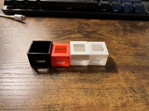
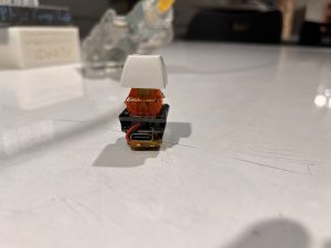
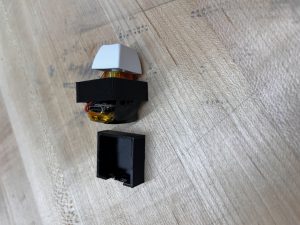
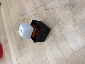
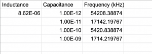
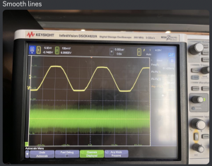
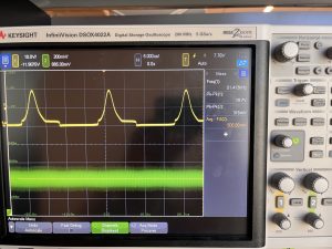
This week was quite a bit of debugging for the inductive charging kits, in conclusion we have determined that the kits are specifically tuned to the inductance and resistance of the kit coils. While understandably so, we have been swapping out the resistors and capacitors on the board to make our own observations on what each component has in relation to the inductance values, in which case we are quite stuck on. The board has capacitors that are not seemingly tuned to resonance so this makes it more difficult to determine what changes are needed to be done.

The inductive kits are made of a power amplifier and an oscillator, we haven’t found a direct relation as to what the changes are. We compared with sample schematics but even when replicating a schematic, it was not attuned to the stated inductance but still to the 30uH. We tested with various resistors, capacitances, and creating new coils.

We may look to buying products that fit our size, but may need to lengthen the housing more, however it would be good to have a meeting in order to sort out what could be done with the pcb kits we have.

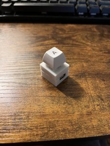
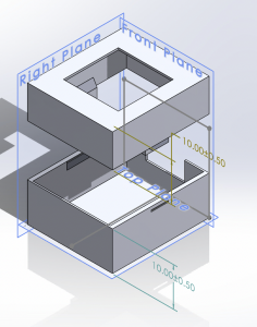
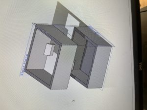
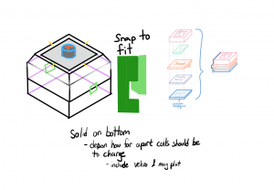
As for 3D housing, because most of time was spent on figuring out the inductive kits, that is a bit behind, but I plan on printing the changes on Sunday. I added the top cover, adjusted the wall widths, added a USB-C hole, and compacted the width of the total housing to be thinner on one side, however, the other will stay the same.

Korene’s Status Report 3/25

3D housing test fitting was completed and started looking over the inductive charging pcb kits.

The fit was well and had suitable tightness for joints and solid feeling. There’s no tilt whatsoever so it’ll be good to continue the design for it. Perhaps it’ll be beneficial to have a wrist rest so users can type at a more comfortable height, however this is nothing new to the keyboard world as many users have wrist rests in order to use their keyboards that may have a slightly higher profile.

Rough changes were made to the 3D housing and we have adjusted measurements for what to change in the next print out of the housing. We shall make 3D housing changes such as a hole for the USB-C port, adjust the height, and account for the receiver charging pcb. We’ll be on track to complete fulfill the requirements for size.

Inductive charging wise, Zhejia and I have identified what is necessary to change in order to adjust the boards for our usage. We were successful removing the current coils on the boards and now going through calculations to get through the correct capacitor values to replace them. We use the reference circuits from before and are able to identify each piece well.

Next week we’ll continue the process. Perhaps a bit slow this week, but we have a plan for next week.

Korene’s Status Report 3/18

This week completed ethics assignment and the 3D housing design in solid works. Unfortunately, this proof does not have screenshots because I had forgotten to take them, but the files are in Box.

It was necessary to spend a while on refreshing solid works knowledge and relearning some shortcuts. I used these tutorials for guidance on snap fit joints and splitting parts

Completing the 3D housing base was relatively simple overall, however, I followed the tutorials above to ensure it would be a smoother process. Still in the progress of making the joints as there are some issues with the joint sketch and extrusion of it. Printing out the joints will also be a different thing as we will have to edit the spacing a few times to ensure a smooth fit.

We also received the inductive charging kit so next week I plan to get a prototype of inductive charging with Zhejia next week as well.

Currently this is good progress made, not stuck on thinking about what parts to buy and we can continue working towards the goal.

Korene Tu’s Status Report 3/11

We’ve decided to buy some new products for wireless charging and in terms of the project we’ll be figuring out the protocols of connecting the keys to the MCU to the computer, in which case more embedded programming is necessary to learn how to clarify and how that works in practice.


Majority of the week was spent on the design review reports and organizing the plan of what we had up until now. Through writing the design review, I figured out where we were in our budget which may be a concern but can now be warier of how to spend our budget. In addition, writing out the whole plan thus far helps to figure out where any more vague plans were vs. what we can easily explain was well thought out.

Afterward, I drafted a drawn plan of the 3D housing for the keys and saw what interlocking method we would use(snap-to-fit cantilever joints), and estimated the size. Overall, in order to have a snug fit we’ll probably have about 5% more room than needed from a tight fit to be looser.

I made a quick table of what capacitors would be needed to have what frequency for the inductor coils which are.


Overall some difficulties are figuring out the microcontroller next and waiting for some parts. Maybe some time crunch but now that we’re over the first half of buying items we can continue onwards.

Korene’s Status Report 2/25


This week was a lot of research into what components to buy. We had the proof of concept from last week but realized finding other components would prove to be a bit more difficult than expected. The first thing was the needed addition of a sine wave oscillator, we thought of a few options: using a Colpitts oscillator, a 555 timer with capacitors to make the sine wave, a VCO, or buying a whole wireless charging IC that would have it’s own pair of receiver and transmitter IC chips to then use and adjust. The problem with a Colpitts oscillator would be the math may not be as accurate, same thing with the 555 timer as it may prove to have slightly off frequency wave generation. In addition, we’ll need a power amplifier to increase the voltage and current output of the wave generated. Finding a good VCO on Digikey was oddly difficult, either needed to buy 50 in bulk or it was still a square wave generator or it ended up being a microcontroller itself. In addition, we’ll need to have something that can generate a specific voltage for that. Zhejia and I have spent most of Saturday and Wednesday searching for different ICs that could fulfill our needs. Most appeared to be much more complex than we needed and take up too much space. We found one that appears to be great for our usage in terms of size and simplicity and is also used quite often in other wireless charging products– XKT-510 for the transmitter and T3168 for the receiver as a pair from Taidacent or P9235 and P9222 from Renesas.

We’re a bit behind due to the unknown factors seen in buying the PCB parts, hopefully by Monday we can decide on a product to run with, and from there we’ll start the PCB schematics.

Weekly Question: enumerate how you have adjusted your teamwork assignments to fill in gaps related to either new design challenges or team shortfalls (e.g. a team member missing a deadline)

Zhejia and I have doubled down on the search to ensure we can figure out what parts we really need. Ben has stayed on track pretty consistently so I’ve mainly been focused on my tasks to come to a decision on parts to resolve the issue.

We shall enter the purchase form next week and I look to have a pcb schematic of parts, perhaps even start on layout and looking into what is needed to fulfill requirements.

Korene’s Status Report 2/18

Over the past week, Zhejia and I have developed the plan for the inductive charging and created the proof of concept circuitry for it. Currently, we are now searching for the specific parts for the rest, but have found the inductive coils to buy (buying because it is more reliable to have the same inductance rating and be more consistent). Photos of the circuitry are on Zhejia’s Status Report. Some unknown results are why the current input and output appear to be so low and when measuring output current the voltage readings on the oscillator become warped. (top picture below is as normal measurement, bottom photo is when we measure for output current)

Next we need to make our calculations based around the 8.32uH inductors and then we can make a base schematic for the PCB. We plan to buy materials at beginning of the week to get them at the end of the week. Then test on the breadboard and complete the schematic and layout of the PCB to be sent out for fabrication(week after getting parts to buy)

We should be on schedule, but in practice a bit late in terms of when to send out a PCB board to fabricate. I hope there is still enough time to order one and then order another just in case.

A lot of 220 is being used here as it provided the best overview of a diverse number of components. We used Lab2a handout to build the full bridge rectifier and voltage regulator and lab4a to build the circuit to measure for resonance frequency. It’s a lot easier the second/third time around and cool to see it used to actually charge inductively! Some 18310 and 18320 knowledge is being used because of knowing about mosfets (and soon 18421 when we start looking at what power amplifiers to use in order to boost our power)

Korene’s Status Reports 2/11

This week I had presented the proposal and rehearsed the speech in order to deliver in an engaging manner and also read through the application notes of several microcontrollers to see what will be the base microcontroller to use for our main pcb. In addition, Zhejia and I researched on inductive vs resonant charging and decided we best make an inductive charging station as that appears to have a more straightforward design. I found a test schematic for Zhejia to then test out to make a proof of concept.

We solidified our plan that the microcontroller be a USB-C that will plug into the computer with ease and that we can just have it run on BLE instead of having the conversion from BLE to Bluetooth, this can reduce latency and switching between too many protocols.

The magnetic charging will require the PCB so it’s debatable on whether we can use that for the hardware component of capstone and or I could focus more on optimizing the space for the key PCBs, I’ll consult with the TAs and faculty on whether this is a good idea. Either way using the NRF52832 will be useful as it’s a small microchip with great specs, speedy and small.

Next week I’ll research harder into how PCB layout works, as that is probably the subject that is of most concern for the keys.

Originally was thinking stacking the key PCB with the SEEED and the magnetic receiver pcb would be enough but I’ll look more into how the connection would work.

This week I did not get as much progress in depth research into the PCB making, but next week shall be full send.

Korene’s Status Report for 2/4

What did you personally accomplish this week on the project?

This week I solidified with my teammates of our project idea and ensuring our project requirements and use case are valid in order to continue. Continuing forward I started researching how Bluetooth Low Energy works in regard to client and server connections. I completed my status report for the week, the team status report, and slides for the proposal

Is your progress on schedule or behind? If you are behind, what actions will be taken to catch up to the project schedule?

Progress is a bit behind in terms of researching BLE  I plan to do more research on how BLE works and also figure out what other footprints would be necessary for the PCB and if we need one. In terms of assignments, I am doing my part to be on track with assignments.

What deliverables do you hope to complete in the next week?

Completing a picture of logistics is crucial and having a draft of footprints and other parts needed in order to also determine how large our keys will end up being.