
Weekly Status Report – 05/04
Bhuvan’s status report (May 4, 2019)
This week, I finished up the final steps of the application layer. Mainly working on last minute testing for the demo on Monday. After the demo will put in the final changes to the design report.
Dhruva’s Status Report (May 4, 2019)
This week, I had the presentation which went smoothly. My work is mostly done. Once Bhuvan is done with the application layer integration, our capstone will be ready for demo.
Raziq’s Status Report (May 4, 2019)
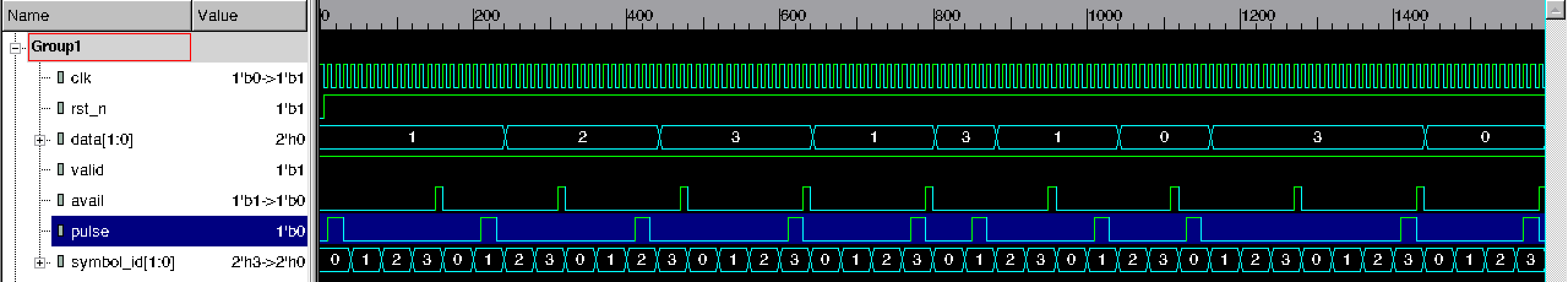
This week has been relatively calm. The datalink layer is pretty much set at this point, and I have identified the necessary parameters to reach our benchmarks. I’ve also helped tweak the digital filtering on the input pins for better accuracy of reception.
Upcoming work
Record and upload demo video
Present capstone demo
Finish and submit final report
Team Status Report
We are working together on completing the remaining deliverables. This weekend will be for wrapping up for the public demo and for recording the video. We have also started the final report, which we will revise on Tuesday and Wednesday before submitting.
Weekly Status Report – 04/27
Bhuvan’s status report (Apr 27, 2019)
This week, I finished implementing the application level. The application layer worked perfectly at slower speeds and received almost 100% accuracy when integrated with the physical layer. The accuracy however drops when changing the parameters of the encoding and decoding to work at higher speeds. My guess is that this is due to the result of adding a timeout which is too small and thus causing the FSMs on the receiver and transmitter sides to go out of sync (ie. the receiver is waiting for DATA packets while the receiver is waiting for READY packets). I also run into issues where the packets coming in between the receiver and transmitter have off by one errors which result in the FSMs not recognizing the packet as a certain packet. I will continue to work on these issues over the weekend. One potential fix for this issue might be to use more loosely defined READY, ACK and NAK packets to offset the off by one errors.
Dhruva’s Status Report (Apr 27, 2019)
This week, I worked on further optimizing distance and speed. This was on the modulation side and the circuit side. I have been changing fixed components in the circuit to see if we can get any improvements on the distance between transmitter and receiver. I also built the main circuit which we will be using for the final demo. In addition to this, I spent time on preparing the slides for the final presentation.
Raziq’s Status Report (Apr 27, 2019)
This past Monday was our in-lab demo. We were asked many questions regarding the performance characteristics of our protocol, some of which we have reflected upon. On the datalink side, I have been performing tests to determine the best parameters for speed and distance. Before the new LEDs came in, we have been able to transmit at up to ~850 Kbps from a few centimeters away. Now I am performing new tests with the LEDs to see if we can break 1 Mbps. Then we will re-integrate the application layer and be set for the demo.
Upcoming work
Integration and bug fixing for demo
Improve speed of data transmission
Team Status Report
We received all ordered components. We are working together on the final presentation and poster, as well as preparing for the public demo.
Weekly Status Report – 04/20
Bhuvan’s status report (Apr 20, 2019)
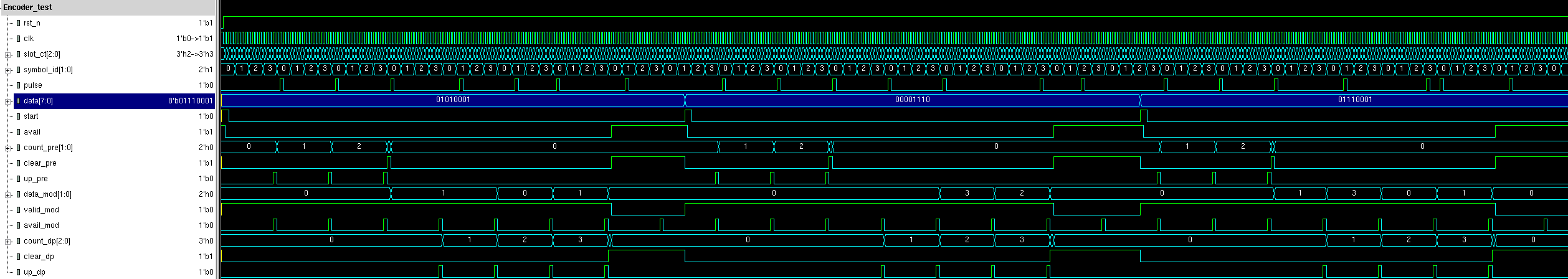
This week, I worked on creating an application level protocol to transfer packets of data across our network. The protocol works with the receiver first sending a READY packet to the transmitter. The transmitter then sends the data packet to the receiver. The receiver must then send an ACK packet to the transmitter to confirm receipt. If the data is corrupted or no packet is sent after the receiver sends a READY, a NAK is sent to the transmitter indicating that the packet must be resent. Currently I am working on fixing minor issues with the packet formatting as we cannot be sure that all bits in the READY, ACK and NAK packets are sent correctly. I am also working on adding a CRC check to the data packets. I will be working with my teammates to iron out bugs over the weekend.
Dhruva’s Status Report (Apr 13, 2019)
This week, I made significant progress on our capstone. The high-speed op amp came in and I integrated that with the circuit. This required some gain changes as well as incrementally modifying resistor values and supply because the new op amp had different characteristics. These changes along with some changes in the verilog modules allowed us to achieve a speed of 600Kbps which is much much larger than what we had originally intended. I also worked on increasing the distance between the transmitter and the receiver. This required the addition of a switching transistor circuit which I designed and integrated. Adding the transistor increased the distance but only slightly. I will continue to investigate the reasons for such a small increase as well as any other avenues of increasing the seperation between the receiver and transmitted diodes. The in-class demo is on Wednesday next week, and I anticipate that the integration with the application layer will be complete by then.
Raziq’s Status Report (Apr 20, 2019)
This week, I worked with Dhruva on optimizing the modulation/demodulation protocol for speed and distance. This was an iterative process involving testing different constant values. The data size (bits per symbol) has been fixed at 2 since for now we do not need to consider multiple concurrent transmissions to the same receiver. Thus, the pulse width and slot size are the primary factors affecting speed and reliability. We have been able to achieve throughput in around 600 Kbps, with slot size on the order of 800 ns. As far as distance, we are working on increasing the distance beyond 3 cm. This involves both the physical and datalink layer. On my side, the primary way is by adjusting pulse width. Currently, the pulse width cannot be larger than the slot size, but this may be modified as needed.
Upcoming work
Integration and bug fixing for demo
Increase distance between LED and photodiode
Improve speed of data transmission
Team Status Report
We received the high speed op-amps and 9V batteries. We are still waiting on the high speed LEDs to be delivered.
Weekly Status Report – 04/13
Bhuvan’s status report (Apr 13, 2019)
Working on our project, with the new scenario in mind, we will have to simultaneously work on increasing the distance and the speed of our protocol. With this change, the current application layer of Pong is meaningless as there is speeds of 1.6kbps are too slow to be comparable with bluetooth. I will be working on restructuring our application layer to show a file transfer test and assist the other team members with the distance and speed aspects as needed.
Dhruva’s Status Report (Apr 13, 2019)
This week as a team , we shifted gears slightly with regard to our project. Instead of setting up a multi node network we spoke to our professor and decided that we needed to change our goals. In our mid point demo, we demonstrated a full duplex communication between the FPGAs. After lengthy discussions, we decided that our revised goal should be to maximize speed of communication with regard to these nodes as well as maximizing distance of separation between them. This modification lends itself more easily to real life scenarios where our project can be applied. So we will not be demonstrating pong but instead we will implement a file transfer test.
This week, I researched on how to make these modifications and ordered the parts necessary to change the circuit accordingly.
Raziq’s Status Report (Apr 13, 2019)
This week I did not make as much progress as normal weeks due to Carnival, but we planned for this. Due to the change in application, the multiple-transmission-capable receiver is no longer necessary, which saves time on my end. I still have to tune parameters for optimal performance and reliability. Pulse width, offset delta, preamble size, and data size will be tweaked as necessary.
Upcoming work
Implement File transfer test
Increase distance between LED and photodiode
Improve speed of data transmission
Check with TA about parts we ordered
Team Status Report
On Wednesday of this week, we talked to Professor Tamal and decided to implement considerable changes to our project. The first aspect to consider was the distance between the LED and photodiode. Presently the distance between the diode and LED is around 5cm. With this distance we achieve near perfect data transmission accuracy. However, there is no viable real world scenario that will make our project feasible. The new scenario we are considering is as follows:
“Build a new form of wireless data transmission that achieves speed which is significantly greater than Bluetooth to be used for close range file transfers”
On Wednesday, we submitted an order for high speed op-amps that will allows us to receive pulses from the photodiode at speeds in the order of MHz. We notified our TA by email but have not received confirmation yet.
Weekly Status Report – 04/06
Bhuvan’s status report (Apr 6, 2019)
After the interim demo this week, I continued to work on Pong. The server module will contain the up-to-date position of the ball and its motion. The server will forward the ball location to the nodes as frequently as possible. The nodes will transmit their respective player 1’s paddle location to the server. The server will then use this data to perform calculations to compute the location of the ball on the next game clock. The server will also transmit the opponents paddle location to each node. The node can use the paddle location of its player 1 and the ball and paddle locations received from the server to draw the screen. I currently have the logic for forwarding implemented but there are a few issues in the math used for converting the motion of the ball between nodes (the ball appears to be on screen for one player but is off screen for the other player).
This week I will fix this issue and begin work on integrating Pong with the encoder and receiver modules. For this I will have to write logic to chop the data to be transmitted into packets and send the correct control signals to the encoder and receiver modules.
Dhruva’s Status Report (Mar 30, 2019)
This week was the mid point demo which went pretty well. We demonstrated a full duplex communication between two FPGAs via the transmitting and receiving circuits we had built as we had promised.
A significant amount of time went in reading for the project management assignment due Sunday. We also spent some time giving feedback as a focus group. Thus, I was not as productive as I had wanted to be.
As for work covered, I decided to use the CRC module that we had implemented as part of an 18-240 lab for our error detection and correction process. I also started the process of building the circuit which will be used for the final demo. The main challenge I encountered was that the receiver node has only one receiving photodiode which needs to get pulses from all the IR LEDs i.e.: 4 different nodes. So the circuit needs to be built such that the LEDs are perfectly aligned and the photodiode is receiving the bits continuously. The alignment is a constant whose optimization is out of scope for our project since we have only one reveiver and transmitter on the hub. In an ideal VLC network, every source of light will act as a hub receiver so the alignment issue will not exist. Thus to combat this, I need to figure out the amount of gain on the hub’s receiver needed such that the furthest transmitter is able to send the bits without errors as well as a optimum orientation so that the transmission is seamless.
Since I had finished some of the previous work earlier than expected, I am still on track with our schedule.
Raziq’s Status Report (Apr 6, 2019)
This week, we completed our Interim Demo on Monday April 1. I am pleased that I was able to demonstrate working duplex communications between two FPGAs. We were able to implement a digital low-pass filter on the GPIO input to prevent unintended edges from appearing in the Decoder input. This and other error handling has made the Decoder more robust.
Leading up to the final demo, there are two main integration-level objectives I want to complete. The first is tuning parameters for optimal performance and reliability. Pulse width and offset delta are related to the physical layer, and preamble size and data size are related to the application layer. In the Design Report, we estimated the best values for throughput, but we will now need to see if this still holds with actual hardware.
The second objective is expanding the Decoder to support multiple transmissions, necessary for the hub. The general algorithm is described in the DarkLight paper, and I believe it is straightforward (though not trivial) to convert the procedural algorithm into a synthesizable design. I’ve started by writing more tests both to aid in development and to clarify the specification.
Upcoming work
Finish and test multiple transmissions with one receiver.
Error estimation and CRC implementation integration.
Figure out the amount of gain on the hub’s receiver needed such that the furthest transmitter is able to send the bits without errors
Figure out the optimum orientation so that the transmission of the 4 nodes is seamless.
Continue integration testing for node-server communications
Work on game server module
Team Status Report
We are working towards our final demo on April 24.
We are on track with our proposed schedule and do not anticipate any delays.
Weekly Status Report – 03/30
Bhuvan’s status report (Mar 30, 2019)
As mentioned in my previous status update, I have put working on Pong on hold. Throughout this week, I have been working closely with Raziq on getting reliable comms between two FPGAs which we will use for our demo on Monday. Each FPGA has both a transmitter and receiver and we send data from the encoder of one FPGA to the decoder of the other FPGA. We are initially performing tests without the LED-photodiode circuit in between the two boards and are directly wiring the GPIO pins together. Once we have reliable comms here, we will proceed to integrate with the circuit. Integrating with Pong will come later after we reliably have multi-way comms working.
One of the issues we run into while integrating the encoder and decoder with the physical layer circuit is bouncing on the GPIO pins that send pulses. Below is a screenshot from signal tap that shows the how the pulse oscillates between 0 and 1 before being set to 1. 
This bouncing causes the edge detection logic to detect multiple edges which in turn causes the decoder to parse wrong information. To fix this issue, I have written a digital filter module in System Verilog which will smoothen the input pulse which will then cause is_edge to only detect the final 0 to 1 transition. This will effectively debounce the inputs received from the GPIO pins. I will continue to work on getting our project ready for the interim demo throughout the weekend.
Dhruva’s Status Report (Mar 30, 2019)
This week, I helped debug the code for the receiver and transmitter modules once Raziq had implemented a basic version. For the demo, I had already finished my work a week back.
The key issue faced was integrating the analog circuit with the FPGA. Our problem was that as the analog output signal of the circuit would take about 30us for an edge transition. During this edge transition period, the digital signal read by the FPGA is essentially undefined. This issue is called debouncing. In order to avoid this, I designed a solution which essentially filters this debouncing by maintaining a counter that saves state of the past values of the signal and once the signal has stabilized (based on some threshold which we set), it outputs the final value. I also researched analog methods to avoid this debouncing. The most effective way is to change to higher quality components and adding an ADC converter. However, since we are able to fulfill our purpose by coding up a filter digitally, we decided against this approach.
In the above graph, the debouncing can be seen for a transition between a 0 to 1 bit. This debouncing causes the receiver to interpret the undefined transition bits as the values being sent which results in incorrect output. This is rectified by the filter I described earlier. This approach does cause some skew in our output, however, it is a constant offset for every transition so it can be safely neglected from the perspective of the receiver.
I also worked on researching robust error detection and rectification modules since we observed that we were experiencing many errors in decoding the sent packets. We are still in the process of estimating the error rate in transmission, however we estimate that 10% of the packets are being sent incorrectly and getting wrongly decoded.
The most effective solution I found was called a cyclic redundancy check which can be pretty easily be implemented by the CRC-32 algorithm. It essentially produces a 32 sized check bit array for an arbitrary sized packet. This check bit array is then sent along with the data and the receiver uses the XOR method to detect the number of bits in the data packet that are incorrect.
Raziq’s Status Report (Mar 30, 2019)
This week has been my busiest yet in terms of hours spent. I completed an initial version of the Decoder module on Monday, and on Tuesday I attempted to test it on the circuit with Dhruva. However, we ran into a range of issues which prevented accurate decoding of the data pulses, so from Wednesday onwards I have been working on implementing these fixes.
Below is a screenshot of a simulated testbench of the combined Encoder/Decoder system. This works as a sanity check for changes made to the Decoder.
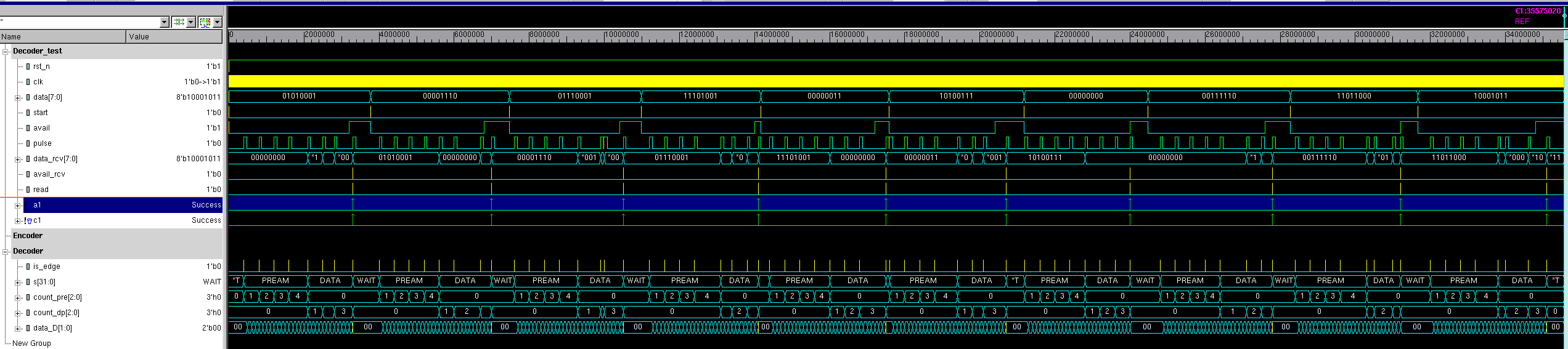
Simulation is all well and good, but there are complications that arise when testing on physical hardware. So, I then wrote a hardware Encoder/Decoder that can be flashed onto the FPGA. One GPIO pin is used to output pulses, and another is used for receiving. I can flash this on two boards to test two-way communications.
Doing this, I was able to diagnose some issues. I implemented basic error detection where if pulses are missed or the preamble is not correctly read, an error is raised. Also, I noticed when I connect the Encoder to the Decoder on the same board, edges are always detected and there are no alignment issues. However, when connected to a different board’s Decoder, there seems to be subtle issues with unsynchronized clocks and with edges sometimes being missed. I’ve asked Bhuvan to look into filtering the GPIO input so that we don’t run into issues such as multiple edges being detected. I also plan to look into analyzing how adjusting parameters like preamble size, pulse width, and slot width affect reliability.
Upcoming work
Finalize demo for two-way communications.
Error estimation and CRC implementation integration.
Start integration testing for node-server communications
Work on game server module
Team Status Report
We are preparing to demo on Monday April 1.
We are on track with our proposed schedule and do not anticipate any delays.
Weekly Status Report – 03/23
Bhuvan’s status report (Mar 23, 2019)
This week I finished implementing and testing the wrapper module that will be instantiated in each node. Presently we do not have comms between two nodes working so to test my code, I wrote a top-level chip interface which displays the screen as seen by each player. On flipping a switch, we can alternate between the two screens. I also started working on the game server which will be the intermediate between the nodes.
I ran into a slight issues where the VGA module would not display on arbitrary monitors but would work flawlessly on the lab monitor. On further debugging, I found out that this issues was caused by the VGA parameters and clock speed. I modified the code to account for this.
The following week, I will be working closely with Raziq to ensure we have working comms between two nodes. This is an important milestone for the demo and I will put working on Pong on hold for a little bit as significant progress was made this week.
Dhruva’s Status Report (Mar 23, 2019)
This week, I spent time working on evaluating the power requirements for the entire project. Components that require power include the FPGA which will be attached to a wall power supply, the monitors on which the nodes are running which will also be connected to wall supplies and the op-amp in the trans-impedance amplifier which requires a steady DC supply. Initially we were planning to use the power supply from the FPGA and planned to build a circuit which would create the difference of a +9V & -9V. I did some research into this and found that using batteries would be simpler and reduce circuit-component overhead. Thus the way I decided to generate +9V & -9V is by attaching the cathode and anode of two 9V batteries which would result in a voltage difference of 18V between the unconnected terminals and the connected node would act as common ground for the circuit. Thus we would also have to factor in the cost of 10 9V batteries in our budget, which is ok because we are currently only using approx. $30 of our budget.
I also worked on breadboarding the 2 circuits for the mid-point demo which is in a week. The circuits have been built and need to be tested with the various validation mechanisms that we used to test the first iteration of the transmitting and receiving circuit. This takes some time because a significant time goes in setting up. I also thought that for the mid-point demo, it would be prudent to have the circuit breadboarded rather than soldered onto a protoboard. This will enable us to make changes if required depending on how we write the demodulation code.
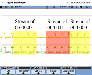
In addition to the above two tasks, I also helped Raziq with the encoding and decoding modules. We were able to successfully complete the encoding module and it seems to be working as we expected. We connected it to the original circuit we had build before the spring break and observed the output on the oscilloscope. We also ran some qualitative tests and measured the skew in the circuit with the encoded data. For the purpose of the test, we sent a stream of 0b’0000 & 0b’0011 which can be observed in the oscilloscope screenshot
.
For next week, I plan to have the 2nd set of transmitter and receiver circuits completely tested so that it is ready to be used for the demo.
Raziq’s Status Report (Mar 23, 2019)
After a relaxing spring break, I got back into work on our capstone. I’ve made a slight reordering in how I will progress, but nothing that will delay any milestones. The decoding and demodulation are too interlinked to be feasibly worked on independently, so I’ve developed the OPPM modulation and encoding modules first. “Encoding” for now is simply dividing up packets of data into a series of consecutive pulses. Preamble 0-data pulses are transmitted before each packet so the demodulation/decoding can pick up on the beginning of the packet (as well as the transmitter’s rise edge offset).
Below is a waveform of the OPPM Encoder being tested (1-tick pulses, 2 bits per pulse, 4-tick slots, 8-bit packets, 3 preamble pulses):
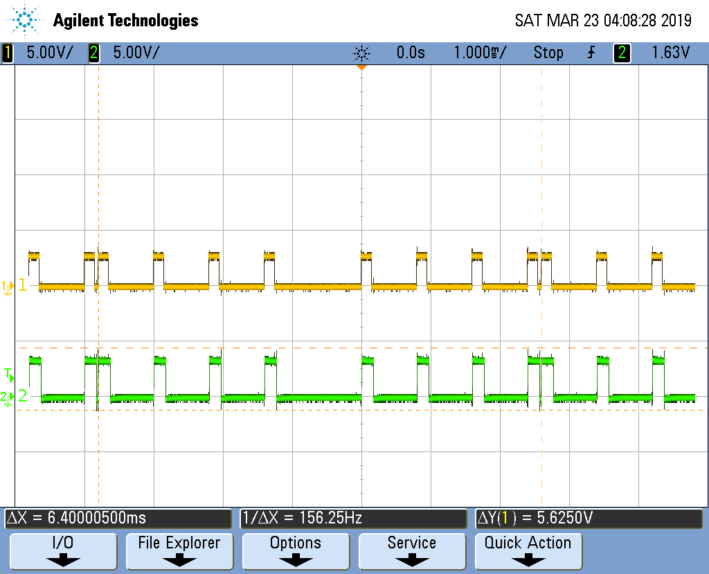
Next, I did some early integration work with Dhruva to make sure that the pulses could be accurately transmitted through the transmitter and received. Below is one transmitted and received packet (yellow measured at the GPIO output, green measured at the receiving end). Because of the limited BW-gain product of the op-amp, we tested with a pulse width of 150us and a slot width of 200us. Other parameters: 2 bits per pulse, 8-bit packets, 4 preamble pulses. The displayed packet is 0b11111111, so three 0b11 pulses were sent after the preamble.
I am currently working on the decoding/demodulation aspect. I will start with a simple simulation-ready version and then expand to add various forms of error handling and robustness.
Upcoming work
Test circuits before demo.
Finish and test decoding/demodulation modules.
Integrate demodulation modules with the circuits.
Start integration testing for node-server communications
Work on game server module
Team Status Report
We will focus more on getting our demo presentable the coming week.
We are on track with our proposed schedule and do not anticipate any delays.
Weekly Status Report – 03/09
Bhuvan’s status report (Mar 9, 2019)
This week, I completed my parts on the Design report and started work on coding the wrappers modules for Pong. I did a little cleanup on the existing code to make it more parametrizable as the existing code makes use of a lot of magic numbers. On playing around with the speed of the ball and paddle movement and refresh rates, I observed that the optimal user experience is obtained when the paddle and ball move 10 pixels per button press and the positions are updated every 2^21 ticks of the 50 MHz clock. This translates to a screen update rate of 23.8Hz. I will continue work on cleaning up the existing code and begin implementation of the wrapper modules to allow networking.
Dhruva’s Status Report (Mar 9, 2019)
This week, I completed the my parts of the Design Report which mainly included the circuit side of the project. I completed sections relating to the approach, implementation plan & validation plan in relation to the receiver and transmitting circuits. I also finalized the parts we would order, the parts we would take from labs, and the components we would assemble ourself. For the purpose of our project, we are primarily assembling all the parts of the circuit ourselves because we found it gives us more control over the voltage levels which we would need to translate into a precise digital signal for the FPGA. I did not achieve as much this week because I had 4 midterm exams during the week after the due date of the design report. However, in my schedule I had planned for this so I am still on track with my work.
Raziq’s Status Report (Mar 9, 2019)
This past week, I completed my parts of the Design Report and started work on coding the modulation and demodulation modules. I’ve realized that this may take longer than just the one week allocated, but the testing tasks can be completed during development, so I still expect to be on schedule. I also have some free time during spring break which I plan to devote some of to capstone.
The OPPM modules will be parametrized in case we need to tweak certain constants. However, for now we expect to use the following values: 8-bit data chunks, 16.22us slot width, 4.15232ms symbol width. The FPGA has a base 50MHz clock, so 16.22us = 811 ticks. Using the PLLs on the board would allow us to implement the modulation without counters, but the added complexity with using multiple clock domains makes it a much-less-preferred option.
The pulse width is another configurable option, but in OPPM it has no effect on the throughput. This is because within a symbol timeframe, only the rise time of the pulse matters in demodulating. Instead, the pulse width affects the average duty cycle (t_pulse/t_symbol), which determines the distance at which the pulse is detected. The DarkLight researchers were able to achieve ~1m distance with 500ns pulses (0.007%), but we are not restricted to low-power applications so we are free to increase this value in order to achieve higher reliability.
Below is a waveform of the OPPM Modulator being tested (2-tick pulses, 2-bit data, 4-tick slots):
Upcoming work
Enjoy spring break!
Begin proto-boarding transmitter and receiver circuits (5).
Test each circuit individually with the validation plan suggested in the design report.
Finish and test modulation/demodulation modules
Start developing encoding/decoding modules
Start developing wrapper module for Pong
Team Status Report
We met with Professor Tamal on Wednesday and received pointers on what should be included in our project for the initial demo. We might consider, designing the circuit on a PCB and connecting the board directly to all the GPIO pins by using a 32 pin female GPIO connector. Another option he suggested was that we 3D print some placeholders for the proto-boarded circuits.
We are on track with our proposed schedule and do not anticipate any delays.