
Bhuvan’s status report (Mar 23, 2019)
This week I finished implementing and testing the wrapper module that will be instantiated in each node. Presently we do not have comms between two nodes working so to test my code, I wrote a top-level chip interface which displays the screen as seen by each player. On flipping a switch, we can alternate between the two screens. I also started working on the game server which will be the intermediate between the nodes.
I ran into a slight issues where the VGA module would not display on arbitrary monitors but would work flawlessly on the lab monitor. On further debugging, I found out that this issues was caused by the VGA parameters and clock speed. I modified the code to account for this.
The following week, I will be working closely with Raziq to ensure we have working comms between two nodes. This is an important milestone for the demo and I will put working on Pong on hold for a little bit as significant progress was made this week.
Dhruva’s Status Report (Mar 23, 2019)
This week, I spent time working on evaluating the power requirements for the entire project. Components that require power include the FPGA which will be attached to a wall power supply, the monitors on which the nodes are running which will also be connected to wall supplies and the op-amp in the trans-impedance amplifier which requires a steady DC supply. Initially we were planning to use the power supply from the FPGA and planned to build a circuit which would create the difference of a +9V & -9V. I did some research into this and found that using batteries would be simpler and reduce circuit-component overhead. Thus the way I decided to generate +9V & -9V is by attaching the cathode and anode of two 9V batteries which would result in a voltage difference of 18V between the unconnected terminals and the connected node would act as common ground for the circuit. Thus we would also have to factor in the cost of 10 9V batteries in our budget, which is ok because we are currently only using approx. $30 of our budget.
I also worked on breadboarding the 2 circuits for the mid-point demo which is in a week. The circuits have been built and need to be tested with the various validation mechanisms that we used to test the first iteration of the transmitting and receiving circuit. This takes some time because a significant time goes in setting up. I also thought that for the mid-point demo, it would be prudent to have the circuit breadboarded rather than soldered onto a protoboard. This will enable us to make changes if required depending on how we write the demodulation code.
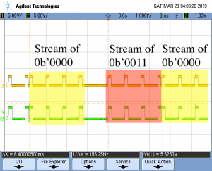
In addition to the above two tasks, I also helped Raziq with the encoding and decoding modules. We were able to successfully complete the encoding module and it seems to be working as we expected. We connected it to the original circuit we had build before the spring break and observed the output on the oscilloscope. We also ran some qualitative tests and measured the skew in the circuit with the encoded data. For the purpose of the test, we sent a stream of 0b’0000 & 0b’0011 which can be observed in the oscilloscope screenshot
.
For next week, I plan to have the 2nd set of transmitter and receiver circuits completely tested so that it is ready to be used for the demo.
Raziq’s Status Report (Mar 23, 2019)
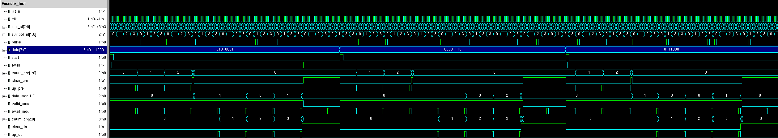
After a relaxing spring break, I got back into work on our capstone. I’ve made a slight reordering in how I will progress, but nothing that will delay any milestones. The decoding and demodulation are too interlinked to be feasibly worked on independently, so I’ve developed the OPPM modulation and encoding modules first. “Encoding” for now is simply dividing up packets of data into a series of consecutive pulses. Preamble 0-data pulses are transmitted before each packet so the demodulation/decoding can pick up on the beginning of the packet (as well as the transmitter’s rise edge offset).
Below is a waveform of the OPPM Encoder being tested (1-tick pulses, 2 bits per pulse, 4-tick slots, 8-bit packets, 3 preamble pulses):
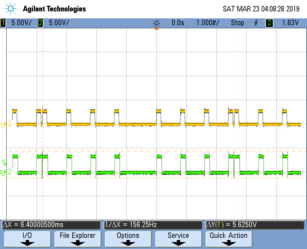
Next, I did some early integration work with Dhruva to make sure that the pulses could be accurately transmitted through the transmitter and received. Below is one transmitted and received packet (yellow measured at the GPIO output, green measured at the receiving end). Because of the limited BW-gain product of the op-amp, we tested with a pulse width of 150us and a slot width of 200us. Other parameters: 2 bits per pulse, 8-bit packets, 4 preamble pulses. The displayed packet is 0b11111111, so three 0b11 pulses were sent after the preamble.
I am currently working on the decoding/demodulation aspect. I will start with a simple simulation-ready version and then expand to add various forms of error handling and robustness.
Upcoming work
Test circuits before demo.
Finish and test decoding/demodulation modules.
Integrate demodulation modules with the circuits.
Start integration testing for node-server communications
Work on game server module
Team Status Report
We will focus more on getting our demo presentable the coming week.
We are on track with our proposed schedule and do not anticipate any delays.