
Bhuvan’s status report (Mar 30, 2019)
As mentioned in my previous status update, I have put working on Pong on hold. Throughout this week, I have been working closely with Raziq on getting reliable comms between two FPGAs which we will use for our demo on Monday. Each FPGA has both a transmitter and receiver and we send data from the encoder of one FPGA to the decoder of the other FPGA. We are initially performing tests without the LED-photodiode circuit in between the two boards and are directly wiring the GPIO pins together. Once we have reliable comms here, we will proceed to integrate with the circuit. Integrating with Pong will come later after we reliably have multi-way comms working.
One of the issues we run into while integrating the encoder and decoder with the physical layer circuit is bouncing on the GPIO pins that send pulses. Below is a screenshot from signal tap that shows the how the pulse oscillates between 0 and 1 before being set to 1. 
This bouncing causes the edge detection logic to detect multiple edges which in turn causes the decoder to parse wrong information. To fix this issue, I have written a digital filter module in System Verilog which will smoothen the input pulse which will then cause is_edge to only detect the final 0 to 1 transition. This will effectively debounce the inputs received from the GPIO pins. I will continue to work on getting our project ready for the interim demo throughout the weekend.
Dhruva’s Status Report (Mar 30, 2019)
This week, I helped debug the code for the receiver and transmitter modules once Raziq had implemented a basic version. For the demo, I had already finished my work a week back.
The key issue faced was integrating the analog circuit with the FPGA. Our problem was that as the analog output signal of the circuit would take about 30us for an edge transition. During this edge transition period, the digital signal read by the FPGA is essentially undefined. This issue is called debouncing. In order to avoid this, I designed a solution which essentially filters this debouncing by maintaining a counter that saves state of the past values of the signal and once the signal has stabilized (based on some threshold which we set), it outputs the final value. I also researched analog methods to avoid this debouncing. The most effective way is to change to higher quality components and adding an ADC converter. However, since we are able to fulfill our purpose by coding up a filter digitally, we decided against this approach.
In the above graph, the debouncing can be seen for a transition between a 0 to 1 bit. This debouncing causes the receiver to interpret the undefined transition bits as the values being sent which results in incorrect output. This is rectified by the filter I described earlier. This approach does cause some skew in our output, however, it is a constant offset for every transition so it can be safely neglected from the perspective of the receiver.
I also worked on researching robust error detection and rectification modules since we observed that we were experiencing many errors in decoding the sent packets. We are still in the process of estimating the error rate in transmission, however we estimate that 10% of the packets are being sent incorrectly and getting wrongly decoded.
The most effective solution I found was called a cyclic redundancy check which can be pretty easily be implemented by the CRC-32 algorithm. It essentially produces a 32 sized check bit array for an arbitrary sized packet. This check bit array is then sent along with the data and the receiver uses the XOR method to detect the number of bits in the data packet that are incorrect.
Raziq’s Status Report (Mar 30, 2019)
This week has been my busiest yet in terms of hours spent. I completed an initial version of the Decoder module on Monday, and on Tuesday I attempted to test it on the circuit with Dhruva. However, we ran into a range of issues which prevented accurate decoding of the data pulses, so from Wednesday onwards I have been working on implementing these fixes.
Below is a screenshot of a simulated testbench of the combined Encoder/Decoder system. This works as a sanity check for changes made to the Decoder.
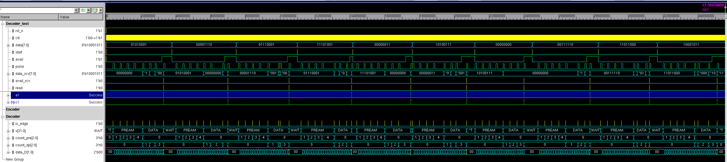
Simulation is all well and good, but there are complications that arise when testing on physical hardware. So, I then wrote a hardware Encoder/Decoder that can be flashed onto the FPGA. One GPIO pin is used to output pulses, and another is used for receiving. I can flash this on two boards to test two-way communications.
Doing this, I was able to diagnose some issues. I implemented basic error detection where if pulses are missed or the preamble is not correctly read, an error is raised. Also, I noticed when I connect the Encoder to the Decoder on the same board, edges are always detected and there are no alignment issues. However, when connected to a different board’s Decoder, there seems to be subtle issues with unsynchronized clocks and with edges sometimes being missed. I’ve asked Bhuvan to look into filtering the GPIO input so that we don’t run into issues such as multiple edges being detected. I also plan to look into analyzing how adjusting parameters like preamble size, pulse width, and slot width affect reliability.
Upcoming work
Finalize demo for two-way communications.
Error estimation and CRC implementation integration.
Start integration testing for node-server communications
Work on game server module
Team Status Report
We are preparing to demo on Monday April 1.
We are on track with our proposed schedule and do not anticipate any delays.