
Bhuvan’s status report (Mar 9, 2019)
This week, I completed my parts on the Design report and started work on coding the wrappers modules for Pong. I did a little cleanup on the existing code to make it more parametrizable as the existing code makes use of a lot of magic numbers. On playing around with the speed of the ball and paddle movement and refresh rates, I observed that the optimal user experience is obtained when the paddle and ball move 10 pixels per button press and the positions are updated every 2^21 ticks of the 50 MHz clock. This translates to a screen update rate of 23.8Hz. I will continue work on cleaning up the existing code and begin implementation of the wrapper modules to allow networking.
Dhruva’s Status Report (Mar 9, 2019)
This week, I completed the my parts of the Design Report which mainly included the circuit side of the project. I completed sections relating to the approach, implementation plan & validation plan in relation to the receiver and transmitting circuits. I also finalized the parts we would order, the parts we would take from labs, and the components we would assemble ourself. For the purpose of our project, we are primarily assembling all the parts of the circuit ourselves because we found it gives us more control over the voltage levels which we would need to translate into a precise digital signal for the FPGA. I did not achieve as much this week because I had 4 midterm exams during the week after the due date of the design report. However, in my schedule I had planned for this so I am still on track with my work.
Raziq’s Status Report (Mar 9, 2019)
This past week, I completed my parts of the Design Report and started work on coding the modulation and demodulation modules. I’ve realized that this may take longer than just the one week allocated, but the testing tasks can be completed during development, so I still expect to be on schedule. I also have some free time during spring break which I plan to devote some of to capstone.
The OPPM modules will be parametrized in case we need to tweak certain constants. However, for now we expect to use the following values: 8-bit data chunks, 16.22us slot width, 4.15232ms symbol width. The FPGA has a base 50MHz clock, so 16.22us = 811 ticks. Using the PLLs on the board would allow us to implement the modulation without counters, but the added complexity with using multiple clock domains makes it a much-less-preferred option.
The pulse width is another configurable option, but in OPPM it has no effect on the throughput. This is because within a symbol timeframe, only the rise time of the pulse matters in demodulating. Instead, the pulse width affects the average duty cycle (t_pulse/t_symbol), which determines the distance at which the pulse is detected. The DarkLight researchers were able to achieve ~1m distance with 500ns pulses (0.007%), but we are not restricted to low-power applications so we are free to increase this value in order to achieve higher reliability.
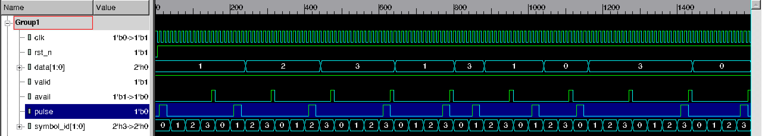
Below is a waveform of the OPPM Modulator being tested (2-tick pulses, 2-bit data, 4-tick slots):
Upcoming work
Enjoy spring break!
Begin proto-boarding transmitter and receiver circuits (5).
Test each circuit individually with the validation plan suggested in the design report.
Finish and test modulation/demodulation modules
Start developing encoding/decoding modules
Start developing wrapper module for Pong
Team Status Report
We met with Professor Tamal on Wednesday and received pointers on what should be included in our project for the initial demo. We might consider, designing the circuit on a PCB and connecting the board directly to all the GPIO pins by using a 32 pin female GPIO connector. Another option he suggested was that we 3D print some placeholders for the proto-boarded circuits.
We are on track with our proposed schedule and do not anticipate any delays.