Jacob’s Status Report for 2/21

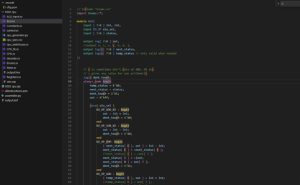
Continued the investigation of the unstable JTAG debug link on the ZedBoard we’ve acquired from the parts list. I’ve tried switching to a Linux dev environment, changing the USB cable, and decreasing the JTAG frequency. But the issue remains unresolved. Given the current status, it is very likely that the issue is with the hardware rather than the setup or software. Instead of continuing to fight an unstable JTAG link on an aging ZedBoard, we’ve decided to purchase two new Arty Z7-20 with the same SoC for our project.

In the meantime, I’ve done some research on the AXI4-Lite we’ll use for interfacing the PS and the PL. I’ve also planned a minimal register map for the interface.

I also presented the design presentation on Wednesday.

Due to the persistent issue with the ZedBoard, a lot of my current work cannot be verified. I plan to use my time during Spring Break to work on the new boards, assuming they arrive on time.
Bert’s Status report 2/21

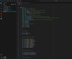
This week, I completed the full RTL implementation of the Ricoh 2A03 CPU core and successfully integrated it with the VCS testbench environment. The entire instruction set has been implemented and passes the primary assembly test suite, confirming baseline functional correctness. In addition, I verified correct behavior across key subsystems including instruction decode, ALU operations, control flow, and memory interface logic.

However, extended validation across several additional test sets revealed edge-case inconsistencies that require further debugging and refinement. Over the next week, I will focus on resolving these remaining issues, improving coverage across corner cases, and strengthening regression stability to ensure robust and cycle-accurate behavior across all validation scenarios.

Michael’s Status Report for 2/14

This week, my primary focus was split between final documentation for our design review presentation and advancing the 2C02 PPU hardware implementation. For the group presentation, I was responsible for drafting the implementation plan and the testing plan, specifically detailing how we will validate cycle accuracy across the CPU PPU interface.

On the technical side, I successfully finalized the Verilog implementation for the background rendering and pattern table fetching logic. This involved mapping the internal VRAM addresses to the pattern table data fetched from the emulated cartridge memory. Additionally, I began developing a dedicated testbench to verify PPU register read/write timing.

I am currently on schedule. Having finalized the background rendering logic this week, I am exactly where I planned to be in our internal timeline. For the upcoming week, I hope to complete finalizing the PPU testbench and verify that register access timing matches the original hardware specifications. In addition, I will begin the RTL implementation for sprite rendering logic, including the priority evaluation for overlapping sprites.

Bert’s Status Report for 2/14

This week, a significant portion of my time was dedicated to the design review presentation. I wrote about our design requirements and the solution approach for the hardware recreation. Regarding hardware implementation, I made progress on the 6502 instruction set logic. Building on last week’s work with bytecode conversion, I have begun writing the RTL for the core execution unit. I have also started setting up the Implementation and Testing plans to verify that our timing remains deterministic as we integrate the CPU with the memory mapping unit.

My progress is currently on schedule. While the Design Review required significant documentation effort, I have maintained the pace for the CPU implementation phase. For the upcoming week, I aim to finalize the initial RTL for the Ricoh 2A03 core instruction set, and run the full suite of assembly tests through the VCS test bench to ensure functional correctness. 

Team Status Report for 2/14

Project Progress Summary

This week, our team focused heavily on preparing for the design review presentation. We synthesized our progress into a cohesive presentation covering our design requirements, solution approach, and implementation plan. Additionally, we continued independent work on the hardware implementation of the Ricoh 2A03 and 2C02 components to ensure our cycle-accurate goals remain on track. 

Risk Management and Schedule

The most significant risk remains meeting the strict timing requirement within our Verilog design to achieve cycle-accurate recreation. As we detailed in the previous week, this can only be fully verified once the CPU design is complete and we perform a formal timing analysis. We are currently managing this risk by adhering to a modular design approach, allowing us to isolate and optimize critical paths early in the implementation phase.

We have made some changes to our design of the multiplayer sync part. Instead of only sending status packets to the second FPGA which only contains the PPU unit, we decide to have the two FPGAs synthesized with exactly the same hardware running the same game simultaneously, and only sync the inputs from the gamepad. Our project remains on schedule. We expect to begin more intensive testing of the custom network synchronization layer once the individual CPU and PPU modules reach their next implementation milestones.

Jacob’s Status Report for 2/14

Implemented bare-metal application flow for game ROM loading and another diagnostic application to test UART. Both are implemented in C and to be run by the ARM core on the ZedBoard. UART has been confirmed to work end-to-end with manual UART byte injection. However, the JTAG/AP debug link is unstable (intermittent AP transaction errors, DAP-only enumeration, e.g. 0x30000021). Because JTAG/AP is unstable, launch/debug outcomes are inconsistent. Software correctness for ROM load and uart_smoke is therefore not yet verified. 

The instability could be due to the current WSL2 dev environment. I’m planning to switch to native linux for another test run. Other potential causes could be the default JTAG frequency being too high, a bad power supply, core overheating, or simply having a defective board (unlikely but possible). Due to the issue described, I am slightly behind the new schedule we drafted. I plan to invest more time to debug the current situation. Once it gets resolved, I’ll continue to work on the rest of the development.

In addition to the above progress and obstacles seen, since I am in charge of the SoC integration, I’ve finalized the design plan using the Zedboard with its ARM core to serve our goal of recreating the NES with remote multiplayer capabilities.


Jacob’s Status Report for 2/7

Since we’ve borrowed ZYNQ-7000 from the provided parts list, we plan to modify our existing plan to utilize the available ARM core on the board. I’ve researched the capabilities of the ARM core and how it can be used for the planned SoC integration.

Specifically, I’ve looked into how to load game ROM files. This will involve using a C library called xilffs on the ARM core to read the .nes file from the SD card. The data will then be pushed from the ARM’s memory into the FPGA’s BRAM using an AXI BRAM Controller. 

I am on schedule (though the specific tasks need to be modified due to the new hardware). Next week, I plan to experiment with ROM file reading, nes file parsing, and data movement with the physical board. 

Michael’s Status Report for 2/7

For this week, I mainly contributed to the proposal presentation slides and prepared for the presentation. On Monday, I presented our proposal to the class. Later this week, I researched on open source information about the implementation of some of the hardware in the NES, such as the 2A03 CPU and the 2C02 PPU. I researched more into the open source implementation of the 2C02 PPU, and worked on extracting and modifying its I/O interface. I focused on extracting the core rendering logic and modifying the top-level interface to support our specific ZYNQ-7000 FPGA pin constraints

I am currently on schedule. According to our planed timeline, I will need to finish the PPU’s pattern table. I have already obtained some data in this regard, and I will finish this in time.

For next week, I I aim to complete the following tasks. I will finalize the implementation of the background rendering and pattern table fetching logic. I will then start on generating a testbench to verify PPU register read/write timing against the 2C02 technical specifications.

Bert’s Status Report for 2/7

For this week, I did some research and study on the 6502 processor and instruction set. I found other open-source projects that have demos on simulation of the processor and attempted to test them on VCS and Icarus Verilog. The main issue that I found and made progress through is how to convert assembly 6502 assembly code to bytecode and provide them to the CPU test bench. I have also studied through the structure of the 6502 processor to understand how the code works.

The progress is on schedule, we plan to complete the main CPU and run tests on those during the first few weeks, what I did is some progress on this step. For the next week, the goal is to run all the tests for the CPU, pass them and try to synthesize through Vivado, and do some timing analysis.

Team Status Report for 2/7

The most significant risk that could jeopardize the success of this project is whether we can successfully meet the timing requirements with our Verilog design. This problem can only be verified once we complete the CPU design, then we do timing analysis on those to see whether it is possible. If that is not possible, we would try optimizing our critical path or we may switch to some other processors. However, switching another processor means we might have to switch the target of the emulation for this project. Currently, we have not planned to make any change to our project design.