Accomplished:
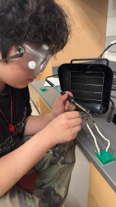
This past two weeks, I spent significant time on both the hardware integration and characterization sides of the project. On the hardware side, I completed the demo PCB layout, finalized the BOM and remaining component selections, submitted the board for ordering, and received both the fabricated PCB and all remaining supporting materials (PCB Components, related demo materials and adapters) needed for assembly on Friday. The hardware side is now largely prepared pending final assembly and the final capacitor value decision. A substantial part of my effort these last two weeks went into pushing the PCB and integration work from the design stage into a physically ready state for the final demo phase.
On the characterization side, I also spent a large amount of time at the probe station finishing V2 transistor sweeps and resistance measurements, then organizing and summarizing that data so it could be directly used for design validation and final presentation work. These updated V2 results were important because, unlike V1, the measured values now fall much more closely within our originally targeted range, which gives us stronger confidence in the current design iteration. In parallel, I also continued helping document the fabrication process in the lab with Ethan by recording footage of the workflow, so we now have a better record of both the fabrication process and the overall project progression. Overall, this week involved a heavy amount of hands-on work across PCB preparation, parts finalization, and measurement-driven validation, which has directly set up the immediate oscillation testing we are beginning tonight after this report.
Progress/Schedule:
I am currently on schedule for my portion of the project. At this point, most of the PCB, BOM, and materials work has been completed, and the main effort is now shifting toward final assembly, presentation preparation, and final verification of the chip behavior. The latest V2 characterization results are encouraging because they suggest the current iteration is behaving much closer to the intended electrical range, which puts the team in a better position going into final presentation week and demo week. With only two weeks remaining, the project is now in its final stage where the priority is making sure the measured data, integration, and final chip behavior all align with the expected oscillator design goals. We are also moving directly into oscillation testing tonight, so the next status update should reflect whether the current iteration is already demonstrating the expected behavior or whether further adjustments are needed.
Upcoming Deliverables:
For next week, my main focus will be helping Charlie prepare the final presentation by organizing the measured data and benchmarked iteration results, especially for transconductance, resistance, and verification that the key design values align with the oscillator conditions we are targeting. In parallel, I plan to solder and prepare the demo PCB so it is ready for final chip integration once the remaining capacitor value is selected. Beginning tonight, I will also support the immediate round of oscillation testing and continue helping verify that the measured behavior matches our expected benchmarks and that we are able to achieve and observe oscillation on-chip ahead of demo day the following week.