Jim’s Status Report for 4/25

Accomplished:
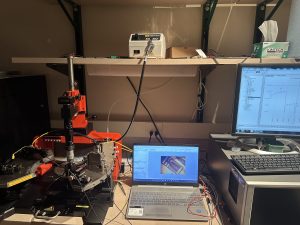
This week, my work focused on final-stage oscillator testing and PCB assembly preparation. During testing, the circuit was able to turn on the LEDs, which was an encouraging sign that the chip and external setup were producing meaningful output behavior. However, confirming actual oscillation remained difficult because the test setup required six delicate probe connections routed into a breadboard. Even very small movements of the wires or probe pins could disrupt the connections, which made it hard to reliably attach the oscilloscope or additional inspection circuitry. We also saw some unexpected test point voltages, but because of the instability of the probing setup, it was difficult to determine whether these came from the device, the circuit, or the measurement setup. On the PCB side, I began soldering and preparing the board for final integration, with the main remaining dependency being confirmation of the final off-chip capacitor values.

Progress/Schedule:
My portion of the project is still moving forward, but the final stage is now constrained mainly by testing and integration limitations rather than material readiness. All PCB materials and supporting components are available, and the board is being assembled while we wait on final capacitor selection. The V2 testing results are partially encouraging because the LED behavior suggests activity, but we still cannot confidently claim stable oscillation without reliable oscilloscope confirmation. The team is also moving into V3 fabrication, which should address the V2 wirebonding issue caused by aluminum adhesion problems. The schedule is tight, but the project is still in a workable position for demo week if V3 characterization and integration go smoothly.

Upcoming Deliverables:
For next week, my main focus will be finishing PCB integration, supporting V3 characterization, and helping prepare the final demo materials. Once V3 is fabricated and wirebonded, testing should become much easier because we will no longer need to rely on delicate manual probing across all six pads. Instead, we can first use our chip holder and breadboard adapter to connect the device into the external circuit more reliably, which should make oscilloscope testing and further voltage inspection much more practical. Once the off-chip capacitor values are confirmed, I will also finish the remaining soldering and PCB integration work. In parallel, I will contribute to the final handout/writeup, poster board, and video so the final demo clearly explains both the design progress and the practical testing limitations we encountered.
Jim’s Status Report for 4/18

Accomplished:
This past two weeks, I spent significant time on both the hardware integration and characterization sides of the project. On the hardware side, I completed the demo PCB layout, finalized the BOM and remaining component selections, submitted the board for ordering, and received both the fabricated PCB and all remaining supporting materials (PCB Components, related demo materials and adapters) needed for assembly on Friday. The hardware side is now largely prepared pending final assembly and the final capacitor value decision. A substantial part of my effort these last two weeks went into pushing the PCB and integration work from the design stage into a physically ready state for the final demo phase.

On the characterization side, I also spent a large amount of time at the probe station finishing V2 transistor sweeps and resistance measurements, then organizing and summarizing that data so it could be directly used for design validation and final presentation work. These updated V2 results were important because, unlike V1, the measured values now fall much more closely within our originally targeted range, which gives us stronger confidence in the current design iteration. In parallel, I also continued helping document the fabrication process in the lab with Ethan by recording footage of the workflow, so we now have a better record of both the fabrication process and the overall project progression. Overall, this week involved a heavy amount of hands-on work across PCB preparation, parts finalization, and measurement-driven validation, which has directly set up the immediate oscillation testing we are beginning tonight after this report.

Progress/Schedule:
I am currently on schedule for my portion of the project. At this point, most of the PCB, BOM, and materials work has been completed, and the main effort is now shifting toward final assembly, presentation preparation, and final verification of the chip behavior. The latest V2 characterization results are encouraging because they suggest the current iteration is behaving much closer to the intended electrical range, which puts the team in a better position going into final presentation week and demo week. With only two weeks remaining, the project is now in its final stage where the priority is making sure the measured data, integration, and final chip behavior all align with the expected oscillator design goals. We are also moving directly into oscillation testing tonight, so the next status update should reflect whether the current iteration is already demonstrating the expected behavior or whether further adjustments are needed.

Upcoming Deliverables:
For next week, my main focus will be helping Charlie prepare the final presentation by organizing the measured data and benchmarked iteration results, especially for transconductance, resistance, and verification that the key design values align with the oscillator conditions we are targeting. In parallel, I plan to solder and prepare the demo PCB so it is ready for final chip integration once the remaining capacitor value is selected. Beginning tonight, I will also support the immediate round of oscillation testing and continue helping verify that the measured behavior matches our expected benchmarks and that we are able to achieve and observe oscillation on-chip ahead of demo day the following week.

Jim’s Status Report for 4/4

Accomplished:
This week, I focused heavily on device characterization and demo PCB integration. A large portion of my time was spent at the probe station performing transistor sweeps, CVU measurements related to switching behavior, and extensive resistance measurements across on-chip structures. This measurement work was important for giving Ethan the empirical data needed to support the V2 design iteration planned for tomorrow. In addition to collecting the data itself, I also spent significant time learning the probe station workflow in practice so that I could more efficiently support characterization needs as they came up.

On the hardware side, I finalized the schematic for the demo PCB this week. With the schematic now complete, the remaining PCB work has shifted from circuit definition to physical layout and packaging in the design software. I was also effectively on call throughout the week to help both Ethan and Charlie whenever new data or measurement follow-up was needed, since characterization results were directly informing design and integration decisions.

Progress/Schedule:
I am currently on schedule for my portion of the project. This week was busy and fairly tight in terms of timing, but it was also productive in that the measurement work successfully produced data that can immediately feed into the next design iteration, and the demo PCB schematic has already been finalized. That means the project has continued moving forward on both the characterization and hardware integration fronts without falling behind schedule. At this point, the remaining PCB work is concentrated in layout, final packaging, and ordering on time.

Upcoming Deliverables:
For next week, my main priority is to complete the demo PCB layout and submit it for ordering by the Tuesday deadline. In parallel, I also need to finalize and order the remaining supporting materials for the demo setup, including items such as the voltage booster (MT3608), chip carrier, and any additional components still needed for assembly and testing. Beyond the PCB and parts ordering, I will continue supporting measurement and characterization work as needed so that I can quickly respond to results from Ethan’s end. My main deliverables for next week are to finish the PCB layout, ensure all remaining materials are ordered on time, and continue providing empirical support where needed for rapid iteration.

Jim’s Status Report for 3/28

Accomplished:
This week, I mainly supported the finalization of the oscillator design as Charlie completed and locked the initial implementation. On my end, I did a final round of NMOS data preparation to better organize the distributions of gm​, Id​, and Vth​ across device types, patterns, and chips, which helped provide cleaner support for Charlie’s final parameter selections and also the W/L dimensions for Ethan to fab. On the hardware side, since the core oscillator test PCB work on my end was already completed, I shifted my focus toward planning the demo PCB, including the supporting infrastructure such as regulators, routing, and other connections needed for a working demonstration setup. I also began preparing for next week’s interim demo and coordinated plans for Sunday/Monday measurements (pending Hackerfab personnel availability as they hold the chip and want to participate in measurement process as well) so that we can begin initial characterization as soon as possible.

Progress/Schedule:
I am currently on schedule for my portion of the project. The main blocker from last week was the unfinished oscillator design and the resulting uncertainty around pin assignment, but now that Charlie has finalized the initial design and Ethan has completed fabrication on Friday, that dependency has largely been completed. As a result, I can now move forward on finalizing the oscillator pin layout and integrating the chip-specific details into the PCB work that had previously been waiting on the completed design and fabrication. 

Upcoming Deliverables:
For next week, my main priorities are to carry out the initial measurements and characterization work, finalize the oscillator pin and layout decisions now that the design is complete, and work with Charlie to finish the demo PCB so it can be ordered on time. Since the base test PCB work is already done, the remaining PCB effort is mainly integrating the finalized oscillator design with the additional support circuitry required for the demo platform. In addition, I will continue to help prepare for the interim demo by contributing to the presentation flow, script, and any technical summaries taken from our empirical measurements.

Jim’s Status Report for 3/21

Accomplished:
This week, I spent most of my time revisiting our NMOS measurement dataset after Charlie shared his schematic. I compiled the key device datapoints and graphs needed to support his design decisions, including comparisons of Id, gm​, and Vth​ across patterns and chips so that we could better choose the most appropriate NMOS pattern/chip combination for fabrication and design. This analysis was important for narrowing the device assumptions used in the oscillator design. For a very general overview and summary of the data I was working with closely, this linked figure shows the scatter distribution with IQR of  Id, gm​, and Vth for our decided Chip 19 across the different NMOS.

On the PCB side, I finalized the testbench PCB design framework. I also selected the PLCC28 through-hole socket as the base component for the demo PCB, and I took responsibility for ordering both the PLCC28 chip holder and a backup PLCC28-through-hole to DIP-28 socket for initial bring-up and contingency testing.

Progress/Schedule:
I am currently on schedule for my portion of the project. The main bottleneck on the PCB side is now the final pin assignment, which depends on Charlie finishing the oscillator design. Aside from that dependency, I have completed the main tasks currently on my end and have been able to respond quickly to Charlie’s requests for measurement data and device-level analysis.

Upcoming Deliverables:
For next week, my role is mainly to remain available on an as-needed basis in case Charlie needs any additional measurements, summaries, or device data to support final design decisions. On the PCB side, the test PCB is effectively complete aside from the final pin assignment, so my remaining work there is mostly waiting for that design information before I can finish the chip-specific integration. In parallel, I will also continue thinking through the other supporting components needed for the demo PCB so that I am ready to move once the final design details are locked in. In addition,  I will coordinate with the team to think about the interim demo presentation.

Jim’s Status Report for 3/14

Accomplished:

This week, I continued working on the test and measurement infrastructure side of the project by drafting the test bench PCB and preparing for eventual integration with the oscillator design. Even though the final oscillator schematic is still being finalized, this work was still useful because it let me make progress on the supporting hardware and think through the practical constraints that the final design will need to satisfy. In particular, drafting the PCB helped me better understand how the oscillator interface, probing structure, and bring-up flow should be organized once the design is available.

In addition, I also worked on the ethics assignment this week. Although this was separate from the hardware implementation itself, it was still useful in thinking about how our design and characterization workflow may be used by future students and lab users, and how we should communicate the intended use and limitations of the system.

Progress/Schedule:

I am currently on schedule for my portion of the project. I have already started drafting the test bench PCB, which puts me in a good position to move quickly once the final oscillator design is available from Charlie, which is expected by tomorrow or Monday (3/15–3/16). At this stage, the main remaining work on my end is to incorporate the finalized oscillator design into the PCB and then push the design toward completion.

In the meantime, I have been using the available time to prepare as much of the test infrastructure as possible in advance so that I can accelerate once the oscillator implementation is finalized. I have also started thinking ahead about the demo PCB, although that work still depends on the final oscillator design and its measured operating behavior.

Upcoming Deliverables:

Next week, my main priority is to incorporate the finalized oscillator design into the test bench PCB and complete that design. My goal is to finalize the test PCB by the end of next week so that it can be ordered on time. In parallel, I also want to continue preparing for the interim design milestone, which is coming up in about three weeks.

If oscillator performance measurements become available soon enough, I will also begin translating those results into early demo PCB planning so that I can start drafting that design as soon as possible. Overall, my focus for next week is to finish the test PCB and prepare the next stage of measurement and integration work.

Jim’s Status Report for 3/7

Accomplished:

This week, I helped complete and submit our final Design Review (DR) report while also continuing work on the characterization and test infrastructure side of the project. A major milestone this week was that we were able to move beyond only having fabricated template NMOS devices and instead begin organizing and analyzing real measurement results from the first iteration, including NMOS I–V behavior, resistor/TLM measurements, and MOSCAP C–V trends. Through analyzing and exploring the data for the DR , I was able to develop better expectations and intuition on how future iteration data exploration and analysis will look like.

In addition, on my end, this was especially useful because it gave me a much clearer picture of the practical electrical constraints that the final oscillator bring-up flow and PCB interface will need to support. 

Progress/Schedule:

We are on schedule overall and have successfully transitioned from the initial fabrication milestone into the first real characterization-to-design loop. Compared to last week, we now have stronger quantitative footing for the project since the measured first-pass device data has started to establish baseline expectations for threshold variation, drive current, leakage, resistor behavior, and MOSCAP behavior. This puts us in a better position to refine oscillator assumptions and make the next iteration more grounded in measured silicon rather than prior estimates alone. We can now progress, as indicated by schedule, on finalizing a potential oscillator design. 

Upcoming Deliverables:

Next week, my priorities are to continue supporting device characterization where needed given fabrication-resulting data, help narrow the practical oscillator bring-up requirements based on the measured data, and resume more direct progress on the PCB/test interface with these updated constraints in mind. By the end of next week, we should be in a position to more confidently lock the initial oscillator implementation direction and translate the current characterization results into concrete testbench and integration decisions for the next phase of the project.

Jim’s Status Report for 2/21

Accomplished:

This week, we completed our design review presentation as well as the first iteration of fabrication of our template NMOS. I had a main stake in creating the presentation along with Ethan, and in parallel continued my personal progress of developing the test and demo PCB for the final oscillator. On my end, I have refined my PCB draft for bring-up and characterization of the oscillator. However, this will be temporarily put on hold as the main focus has shifted to testing and characterizing the newly fabbed NMOS Templates so that Ethan have feedback for v2 iteration on the template NMOS, and that we can start beginning to develop a baseline specs on the oscillator design and performance yields. 

Progress/Schedule

We are just on schedule with our initial February/pre-spring break schedule with our first iteration NMOS fabbed done Feb 19th. As such, we are well within our timeline to progress into the characterization phase of this iteration.

Upcoming Deliverables

Given scheduling conflict, we won’t be able to conduct the characterization earlier within this week. However, we will be able to bring-up, test, characterize, and produce quantitative metrics and specs before the end of next week. By the end of the week, to remain on schedule, we must fully wrap up the first iteration on the template NMOS and give Ethan feedback on the NMOS behavior and specs so we can start the second iteration on NMOS as soon as possible. In parallel, we must also work and produce a final presentable design review report by 2/27.

Jim’s Status Report for 2/14

Accomplished

This week, progress on the physical device was mainly on the fabrication side. Ethan completed an initial template NMOS iteration but the batch did not work out, so the team is restarting the fab run. In parallel, since we are far from creating the final oscillator to test/measure yet, I continued my own schedule in advancing the first draft of the test/measurement infrastructure PCB design for the full oscillator. This is specifically targeted towards bring-up and characterization when the final oscillator is fabricated. Note that for measuring and characterizing the NMOS template, the Hackerfab internal tools suffice by themselves. 

Progress/Schedule

We are still on schedule overall. Despite having to restart, the fab timeline is still feasible referring to the Feb. 19 latest completion date set during the 2/7 team status report. Ethan is projecting to finish another batch before that, so this fabrication reset is possible. For my schedule, my PCB work is proceeding in parallel as I have already completed a rough first draft of the design. There is no pressure/rush on my end for now given the emphasis on fabricating and in-house characterizing the NMOS, but I do need to update and keep the PCB design flexible/modular so we can quickly incorporate any new constraints and updates from the fabrication process.

Upcoming Deliverables

Next week, I will refine the PCB draft into a more complete first-pass plan and align the PCB interfaces for any updates and new constraints reported from the fabrication process. In addition, since the fabrication for the template NMOS is projected to be done soon, I will have to go to Hackerfab and help bring-up and characterize the NMOS and help the team plan for the next iteration.

Jim’s Status Report for 2/7

Accomplished

This week, I focused on preparing our project proposal presentation materials and helping the team communicate and craft a clear initial project timeline. I led and created the majority of the proposal slide deck, namely the slides on use-case, use-case requirements, technical challenges, iterative workflow diagram, and project management plans. On Wednesday, I presented the proposal on behalf of the team to our assigned professor lead and TA. I also began scoping the requirements for the test/demo PCB that I will own (interfaces, measurement needs, and constraints) so the PCB design can proceed in parallel while the first template NMOS iteration is being fabricated and brought up for initial measurements.

Progress/Schedule

I am on schedule for our initial timeline. This week’s focus was on fleshing out the project presentation and finer details to align with the milestones. With the proposal successfully delivered and with my partner beginning the first template NMOS fabrication process, we are on pace with our planned Gantt chart. I am prepared and set-up to begin deeper technical execution next week while fabrication progresses in parallel to my assigned work scope. 

Upcoming Deliverables

 Next week, I will produce a first-pass draft of the test/demo PCB plan and begin SPICE-level simulations to validate key measurement assumptions (main emphasis on fleshing out the finer technical details on loading/buffering and power delivery considerations). Note that although early measurements can leverage existing HackerFab tooling for the first template NMOS characterization, a well-defined PCB test harness will be crucial for repeatable characterization and later iteration bring-up/demonstration on the full oscillator.