https://www.youtube.com/watch?v=3HcLRrBb7zM
Carnegie Mellon ECE Capstone, Spring 2022; Tom Scherlis, Sam Zeloof, Graham MacFarquhar
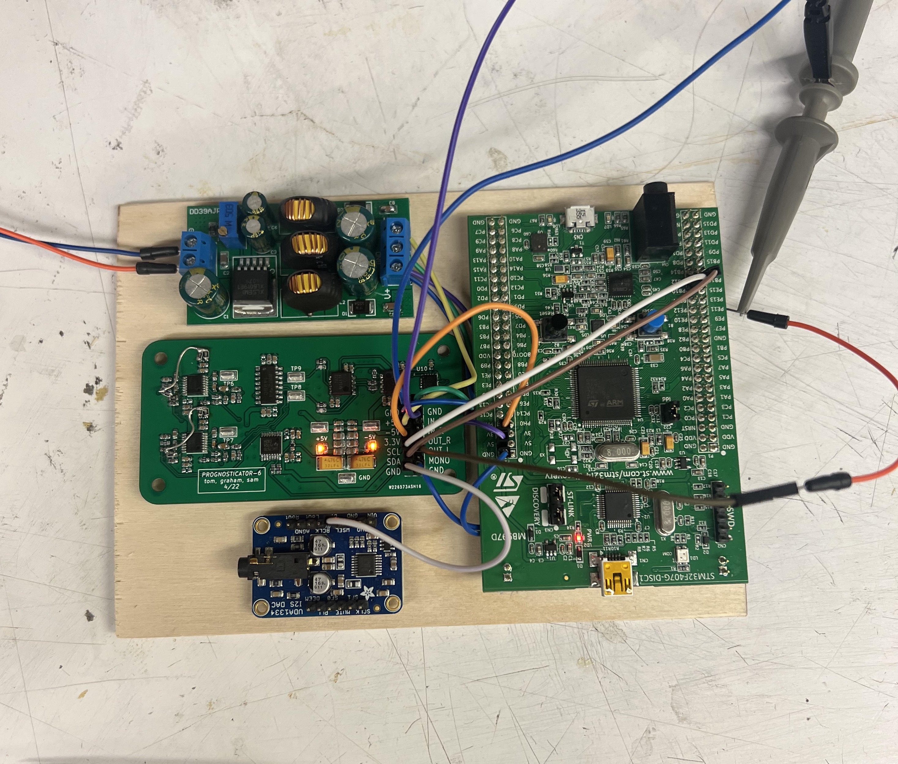
This week I made significant progress on the electronics. The filter board has been completely tested and is ready for integration into the synth. I built a testbench using an STM32 and I2S DAC to drive signals into the analog board for testing purposes:
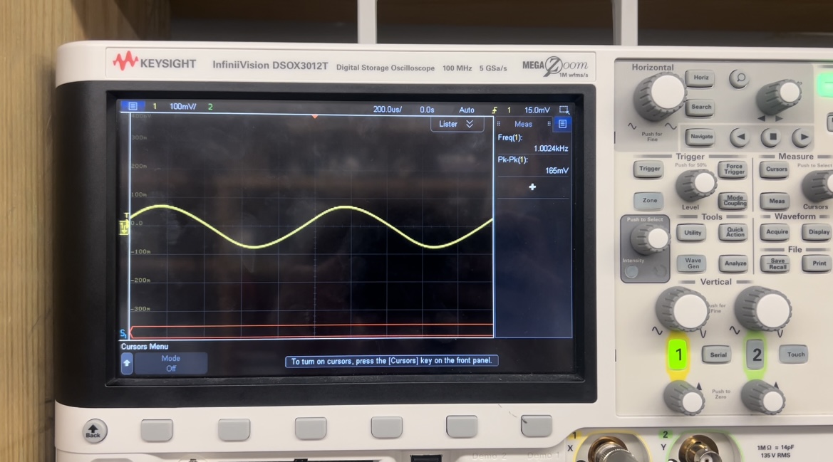
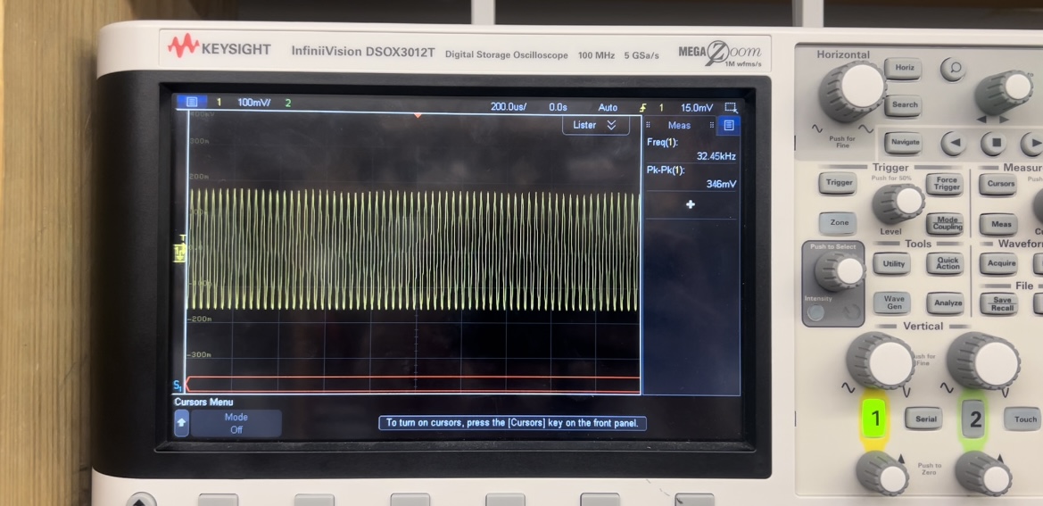
I was able to measure noise, channel matching, filter cutoff performance, and total harmonic distortion.
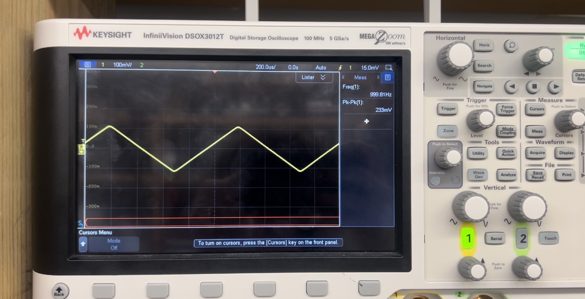
Here’s a test with triangle wave input. The first image is input, second is low pass filtered (higher harmonics removed), and third is with 60dB resonance (higher harmonics and resonance added back.)
In the final week, I will integrate this with the rest of the synth and connect it to our final microcontroller choice (Teensy 4.1). The main deliverable this week is oscillator code written in C to drive this board and also verify functionality after it’s completely integrated. We are still about a week behind in schedule, but given that we have no classes this week will still be able to get everything done.
Last week I had ordered the PCBs and said that to stay on schedule I should have assembled boards by the following week (right now). Luckily, the PCBs arrived a little earlier than expected!
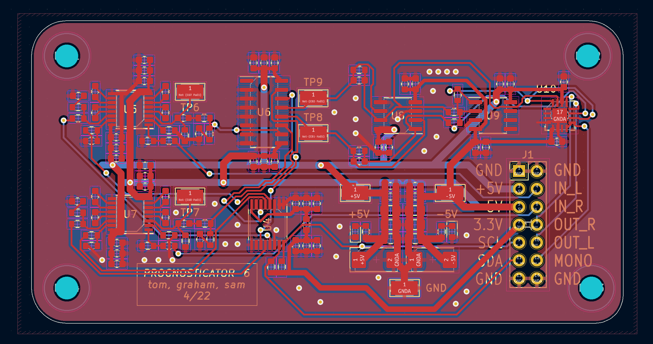
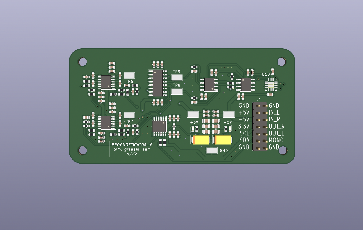
Everything looks great and they passed basic electrical tests (power rails not shorted, etc.) Since the Mouser and Digikey BOM arrived a few weeks ago, I stenciled the board with solder paste, placed all the components, and reflowed it. There were a few shorts and tombstoned capacitors that I had to fix manually, but the finished board looks great:
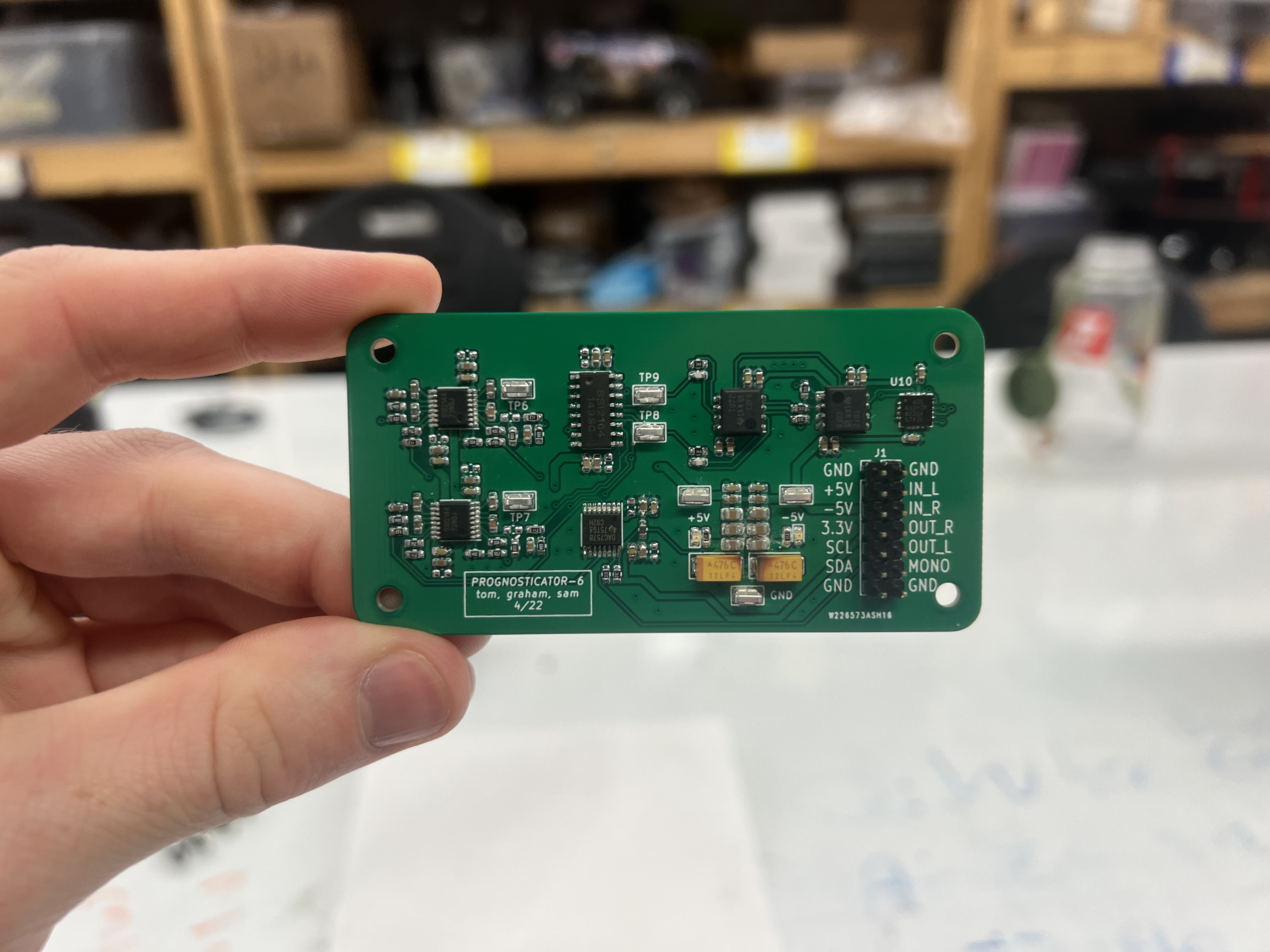
Bring-up was smooth and it’s ready to be fully tested now. I forgot to order 0603 10uF capacitors so there are some un-placed footprints on the board but these are just decoupling capacitors and there is ample capacitance even without those so I don’t foresee any issues. I’ve tested all the basic functionality (control signal DAC via i2c, filters, amplifier) including adjusting filter resonance and cutoff. Everything is working and now I can fully test/characterize it and generate bode plots of the filter response.
This puts us about a week behind, which should be OK because we have a lot of momentum now to push through the final bit of the project. To finish up, next week the deliverable should be a fully tested analog board and integration with the microcontroller.
I have completed the PCB layout and ordered the boards from PCBWAY in China. It’s a fairly small 2-layer board with typical design rules and about 100 components which will allow the board house to manufacture it quickly (2 days) and us to solder everything in a few hours.
The chip shortage has caused a number of the components to go out of stock while I was laying out the board causing me to start over. Luckily, we were able to get the whole BOM finalized and ordered for this PCB layout. All parts, including filter ICs, are in-hand. Once the PCB arrives, we can solder all the components (reflow with stencil) and begin bring-up and testing.
Laying out the board took longer than expected and put us a little more than a week behind. To get back on schedule, we need to have the board in-hand by the end of this coming week and verify that all the component footprints are correct. The main deliverable for next week should be a soldered PCB that is ready for testing and integration into the enclosure.
Last week I said that to get back on schedule I would need to create the finalized schematic, component footprints, and BOM. I’ve done all of this as well as ordered the BOM and begun PCB layout.
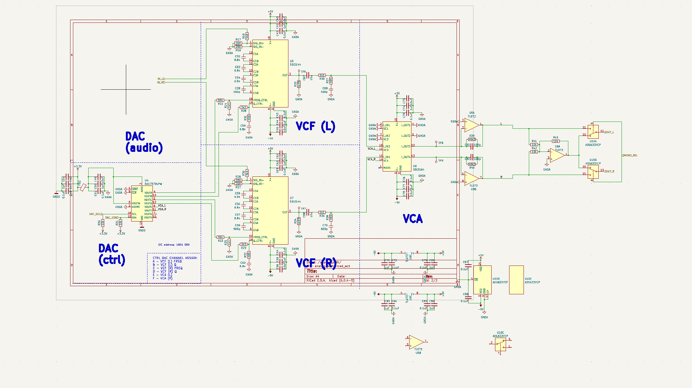
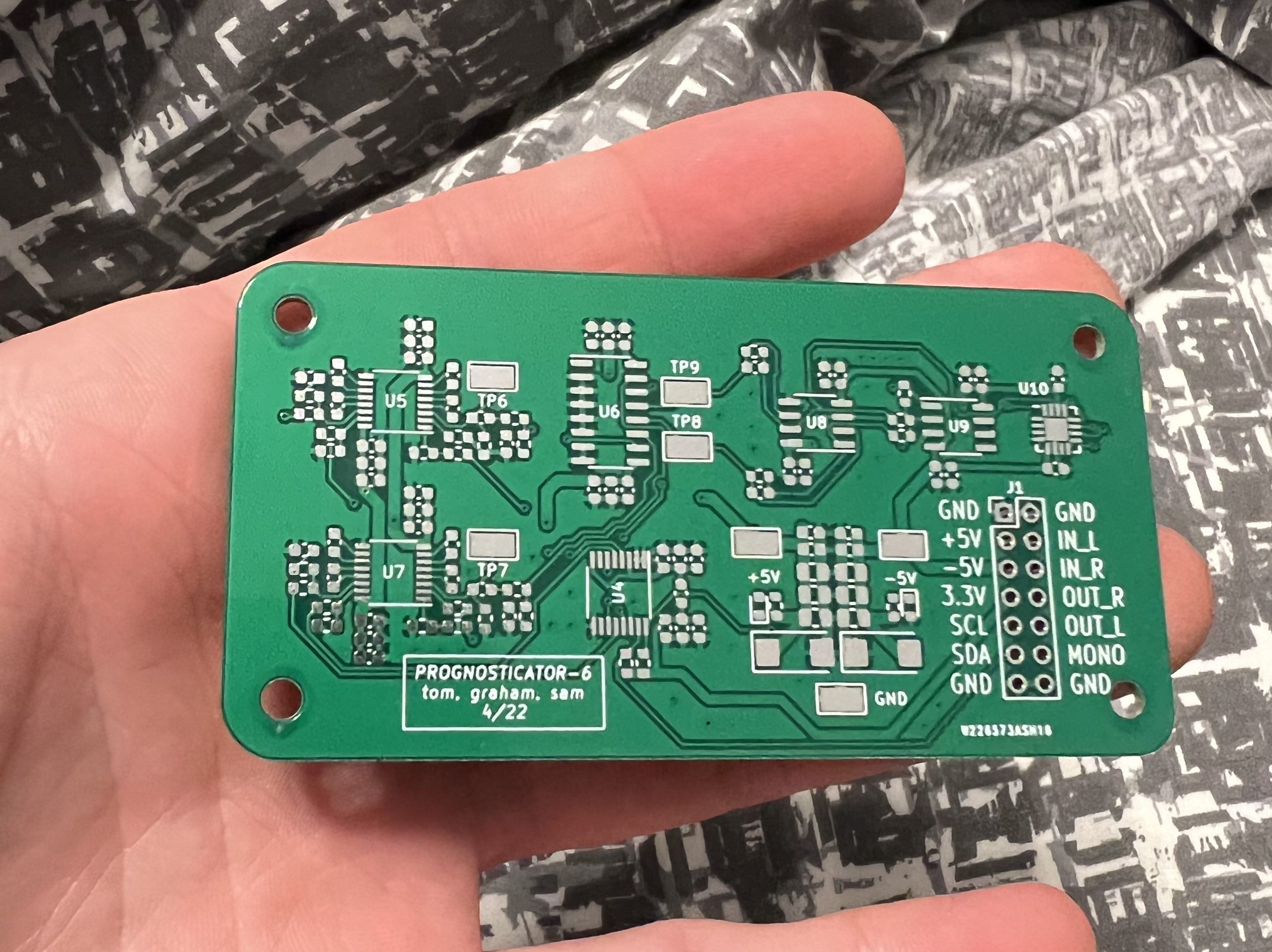
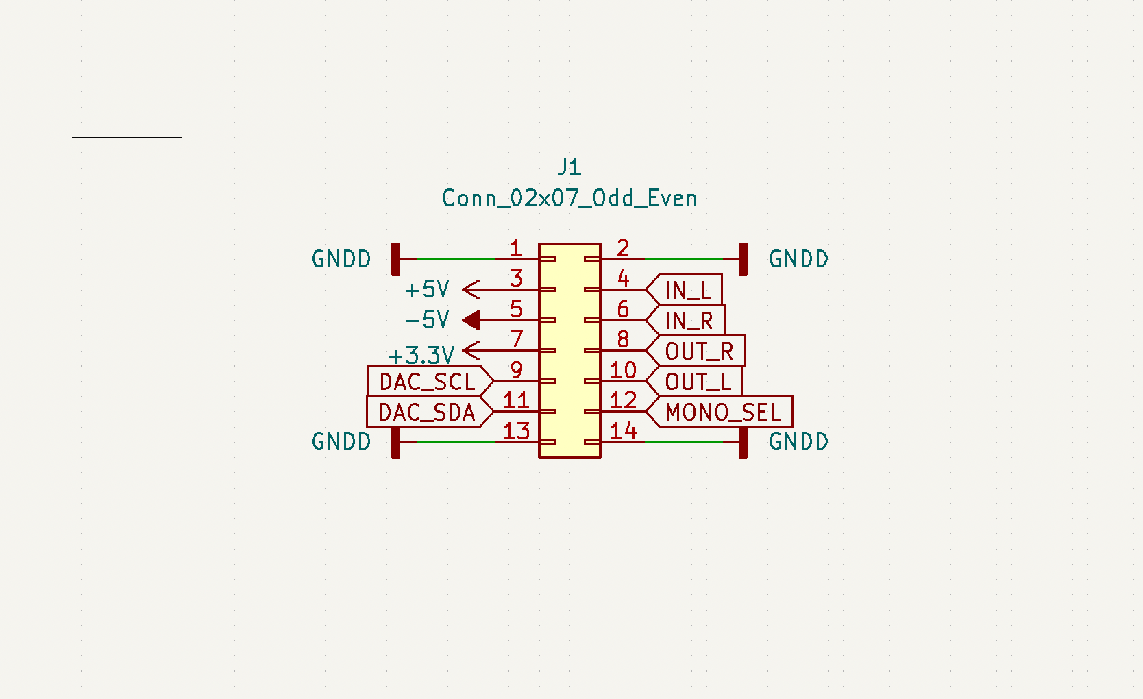
The final schematic does not include an I2S audio DAC as we will use an external DAC breakout board from Adafruit for this. Since this is a 2 channel synth, we want to give the user the option to select for either true stereo output or sum them together in analog for a mono output. I added some circuitry on the right side of the schematic to accommodate this:
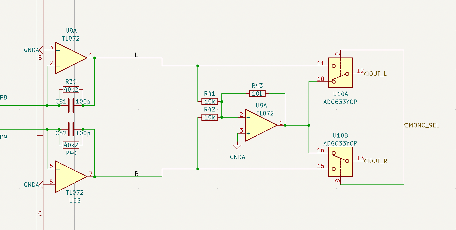 Two (right, left) audio signals enter on the left and are buffered. Then, they a bidirectional analog switch mux IC (U10) either selects the raw buffered signals or a summed version at the output of U9. OUT_L and OUT_R are then sent to the rear panel audio jacks. MONO_SEL is the mux control signal.
I have also begun the PCB layout. This puts us almost on time, but still lagging a little. For next week, I need to complete the entire PCB layout, pass DRC, and prepare to order it from PCBWAY.
This week I went back to the schematic design for the analog PCB and redesigned the interface. Since we may switch FPGA boards (PYNQ-Z2 to Ultra-96) to have better documentation and support, it will be beneficial to make the analog electronics more flexible and agnostic of input signal format. So, instead of having a 40-pin header that perfectly matches the chosen FPGA board’s GPIO, I modified the interface to have a smaller header that will not directly connect to any FPGA or microcontroller board but rather can be manually wired to accommodate any digital controller.
DAC_SCL and DAC_SDA are the serial signals to the control signal DAC which drives VCFs and VCAs. MONO_SEL is a control signal that will select between stereo or mono (summing) outputs. And the remaining pins are audio in and out. This simplifies the analog board interface and treats it more as a filter passthrough board.
This backpedaling and questioning if we should change FPGA boards puts about a week behind schedule. To get back, next week I need to finish the stereo/mono summing circuitry and make board design progress. The main deliverable for next week is finalized schematic, BOM, and component footprints.
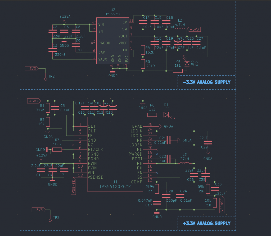
Last week I wanted to finish the power supply section (only the 3.3v rails are done, need to add low noise 5V regulators too) and to get a solid plan for the front panel interface. I accomplished both of these, which technically puts me on schedule. The positive and negative 5V rails are used for the analog path (VCF and VCA both require split rails) and the 3.3V is for logic, FPGA, encoders, etc. We solidified the plan for front panel interface including number and function of rotary encoders. I ordered all the front panel stuff, including knobs, encoders, and quadrature to I2C PCBs. Each encoder will have a small PCB behind it to count the quadrature pulses and put all of them on the same I2C bus which we will be able to poll with the SoC.
Next week, I want to make significant progress in PCB layout. The schematic is becoming more firm and I can start to do actual layout soon. At a minimum, I would like to start the analog path layout next week.
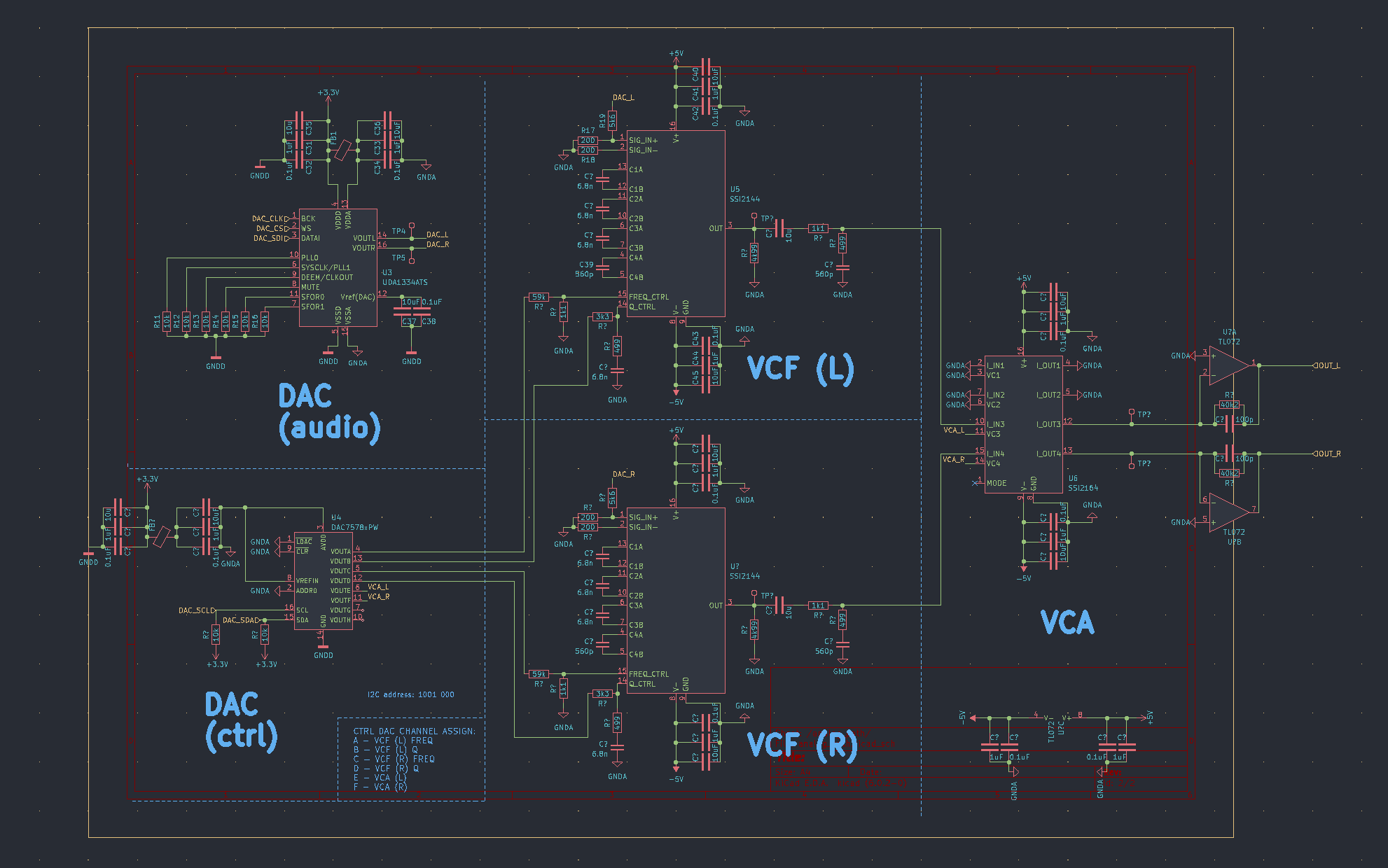
This week, I completed the analog path schematic design which was the goal I stated last week. As a group, we decided to change the synthesizer architecture to be duophonic rather than polyphonic, so there are two VCFs and VCAs with independent control signals. I added ample power supply decoupling and RF chokes to separate the analog and digital supplies. There is a high speed I2S DAC for audio which has two channels (right, left) followed by two VCFs with both adjustable cutoff frequency and resonance, then two VCAs. The output of the VCAs is buffered with opamps and an 8-channel I2C DAC is used to generate the control signals which drive VCFs and VCAs.
Completing this puts me perfectly on schedule, which is great. For next week, I want to finish the power supply section (only the 3.3v rails are done, need to add low noise 5V regulators too) and get a solid plan for the front panel interface. This includes ordering the correct number of potentiometers, rotary encoders, and knobs as well as starting the schematic design.
This week I worked on schematic design and analog filter path design. Our initial project specifications and block diagrams were vague so we worked to solidify those and nail down the specific filter/analog architecture. To save time and help increase the odds of success we traded the discrete switched-capacitor filter architecture for monolithic voltage controlled filter integrated circuits. We will have a low pass filter with programmable cutoff frequency and resonance that are adjusted proportional to a current value that comes from a control signal DAC. There is also a main (I2S) DAC for the audio path. The output of the filter is then fed into a voltage controlled amplifier before the “line out” jack.
The analog path also requires a very low noise split-rail voltage supply. I designed 2 switching regulator circuit that convert a noisy 12V input to +/- 3.3V (extremely low noise). After some research, I decided to separate analog and digital grounds with an inductive choke to connect them.
This is good progress but is about 1 week behind according to our gantt chart. To rectify this, I plan on having a final filter schematic for next week so that I can begin PCB layout ASAP. In the meantime we can also work on sourcing the parts as we will likely need to order from a few different sources.
The project is going smoothly overall and we’ve been working on system level planning like I/O allocation, block diagrams, and front panel layout. Right now it seems like the largest risk that may jeopardize the project is the complexity and number of features that we want to add. A fully featured synthesizer has so many individual features, effects, and subtitles. We have not made any changes to our schedule or planes yet, but may need to slightly reduce scope and define more stretch goals to work on later given extra time.
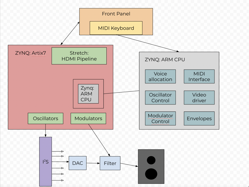
Initial system block diagram:
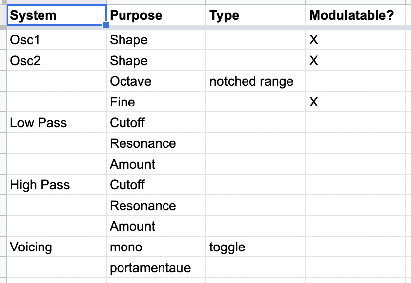
Front panel knob planning: