This week I went back to the schematic design for the analog PCB and redesigned the interface. Since we may switch FPGA boards (PYNQ-Z2 to Ultra-96) to have better documentation and support, it will be beneficial to make the analog electronics more flexible and agnostic of input signal format. So, instead of having a 40-pin header that perfectly matches the chosen FPGA board’s GPIO, I modified the interface to have a smaller header that will not directly connect to any FPGA or microcontroller board but rather can be manually wired to accommodate any digital controller.
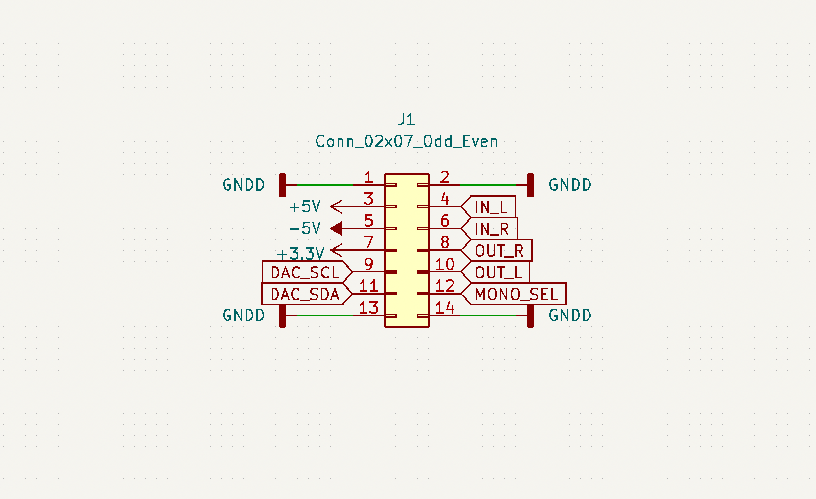
DAC_SCL and DAC_SDA are the serial signals to the control signal DAC which drives VCFs and VCAs. MONO_SEL is a control signal that will select between stereo or mono (summing) outputs. And the remaining pins are audio in and out. This simplifies the analog board interface and treats it more as a filter passthrough board.
This backpedaling and questioning if we should change FPGA boards puts about a week behind schedule. To get back, next week I need to finish the stereo/mono summing circuitry and make board design progress. The main deliverable for next week is finalized schematic, BOM, and component footprints.