Last week I said that to get back on schedule I would need to create the finalized schematic, component footprints, and BOM. I’ve done all of this as well as ordered the BOM and begun PCB layout.
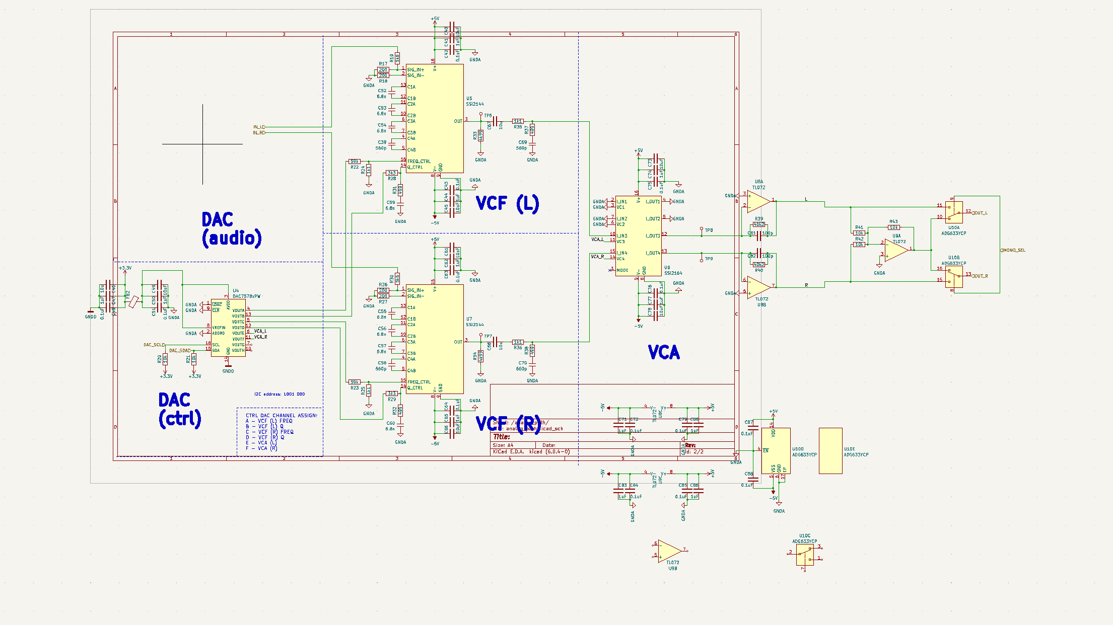
The final schematic does not include an I2S audio DAC as we will use an external DAC breakout board from Adafruit for this. Since this is a 2 channel synth, we want to give the user the option to select for either true stereo output or sum them together in analog for a mono output. I added some circuitry on the right side of the schematic to accommodate this:
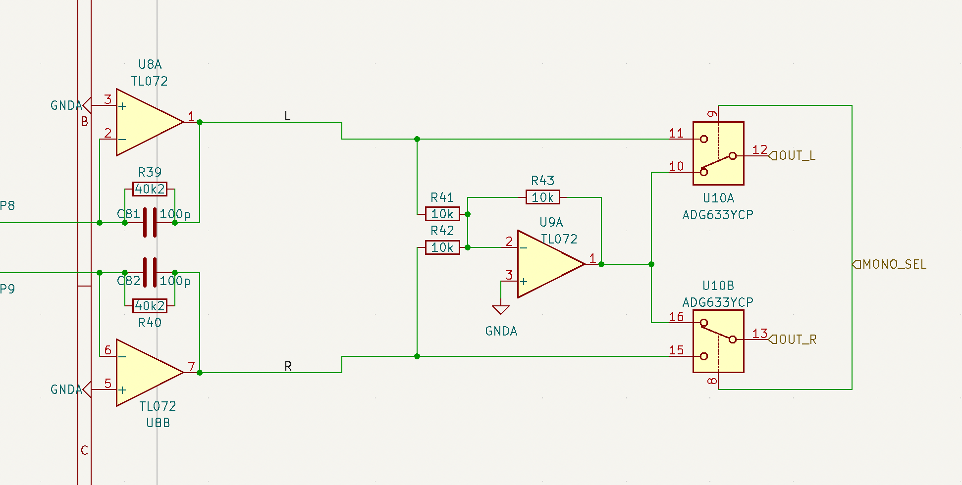 Two (right, left) audio signals enter on the left and are buffered. Then, they a bidirectional analog switch mux IC (U10) either selects the raw buffered signals or a summed version at the output of U9. OUT_L and OUT_R are then sent to the rear panel audio jacks. MONO_SEL is the mux control signal.
I have also begun the PCB layout. This puts us almost on time, but still lagging a little. For next week, I need to complete the entire PCB layout, pass DRC, and prepare to order it from PCBWAY.