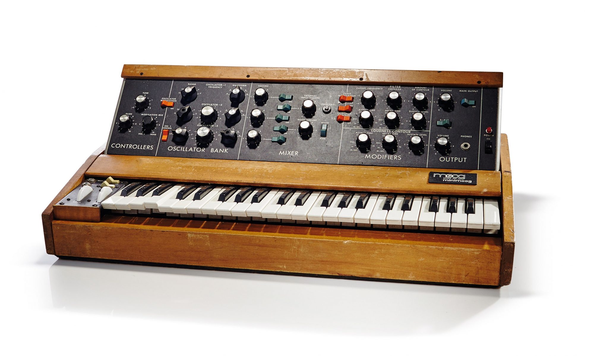
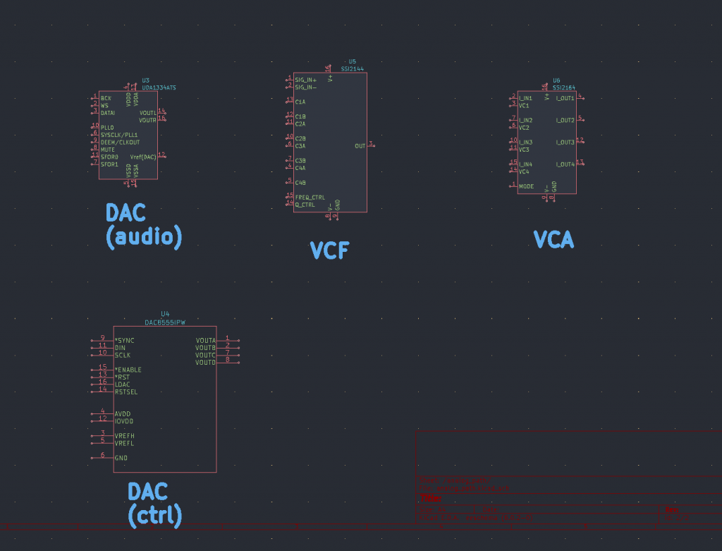
This week I worked on schematic design and analog filter path design. Our initial project specifications and block diagrams were vague so we worked to solidify those and nail down the specific filter/analog architecture. To save time and help increase the odds of success we traded the discrete switched-capacitor filter architecture for monolithic voltage controlled filter integrated circuits. We will have a low pass filter with programmable cutoff frequency and resonance that are adjusted proportional to a current value that comes from a control signal DAC. There is also a main (I2S) DAC for the audio path. The output of the filter is then fed into a voltage controlled amplifier before the “line out” jack.
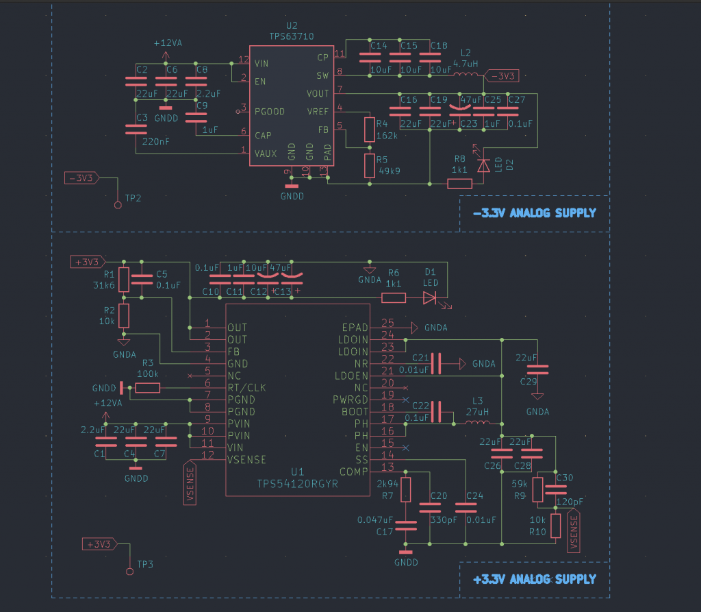
The analog path also requires a very low noise split-rail voltage supply. I designed 2 switching regulator circuit that convert a noisy 12V input to +/- 3.3V (extremely low noise). After some research, I decided to separate analog and digital grounds with an inductive choke to connect them.
This is good progress but is about 1 week behind according to our gantt chart. To rectify this, I plan on having a final filter schematic for next week so that I can begin PCB layout ASAP. In the meantime we can also work on sourcing the parts as we will likely need to order from a few different sources.