This week, we received our FPGA (DE2-115) along with our cameras (OV7670). I spent the majority of the week working on our first task as a team: implementing a PLL on our FPGA to generate the pixel clock for video output to the display. This required me to first set up Quartus and my development environment and also to research how to create PLLs for this specific board. Once I figured all of that out, I was able to implement our MVP output of 640×480@60Hz with a PLL-generated pixel clock of 25.175MHz and a test pattern VGA controller to generate the pixels themselves. Once this was done, Jullia and I wanted to demonstrate that we could extrapolate this design to different resolutions and clock frequencies (our camera needs a separate clock and our goal is 720p60Hz). We were able to prove this as possible by upping the resolution all the way to 1440×900@60Hz with a new PLL-generated clock of 106.47MHz. This was also successful (see photo below), and thus we have successfully mitigated the risks of our resolution being PLL limited. We are slightly ahead of schedule given that we have a sample VGA-controller implemented, and this upcoming week I plan to expand on this by experimenting with the cameras to verify compatibility and remove them as potential risks for the future.
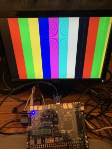
Our test pattern being outputted at 1440×900@60Hz over VGA from our FPGA using a PLL-generated clock of 106.47MHz. Please note that the two off-color blue and green thin vertical stripes on the right are due to defects in my (slightly damaged) panel and are not from our VGA signal.