Joseph’s Status Report for 3/27/21

Since the 13th, I have made some major changes to the PPU task schedule. Due to some design decisions made in the design review report, and most notably our decision to replace our DRAM interface with an M10K VRAM, I have decided to combine the Tile-Engine implementation tasks into a single task, and add several new tasks relating to the PPU FSM.

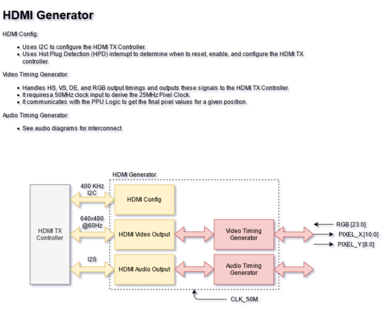
Firstly, due to the new PPU FSM design, I was required to re-implement the HDMI Video Timing. This effectively combines the HDMI Video Output and Video Timing Generator blocks into one custom block. The reason was to gain better access to important signal timings such as DISPLAY, or VBLANK, as well as to read and swap the new row buffer.

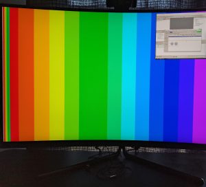
The row buffer currently initializes with a test pattern (shown in the image above). The new HDMI Video Output block reads this buffer for every row. The goal (due next week by Wednesday) is for two row buffers to be swapped in and out, and the PPU-Logic (Tile Engine, Sprite Engine, and Pixel-Mixer) will fill the buffer not in use. The important progress made here is that the HDMI Video Output automatically fetches pixel data in the row, extracts an address from that pixel data to a color in the Palette RAM, and then reads from Palette RAM to obtain the final color. This sequence occurs 320 times in a row, with each result held for an additional 25MHz clock cycle to upscale to 640px resolution.

The next task I completed was the Double-Buffered VRAM implementation. Our VRAM consists of two identical VRAMs, one which is used by the PPU during the DISPLAY period, and one which the CPU can write to during the DISPLAY period. The VRAMs must be synchronized at the start of the BLANK period so that the CPU can write to a VRAM which accurately reflects the changes it has made since the previous frame. The Double-VRAM was implemented using a SystemVerilog Interface to manage all 36-per-RAM signals. The reason there is such a large number of signals is because we use the native M10K dual-port RAM configuration, which allows for an extra port for every signal, and our VRAM is split into 4 segments (each with their own controls). The VRAM Sync is implemented in a new block called VRAM Sync Writer. The VRAM Sync Writer controls all ports of each dual-port VRAM in order to speed up the copying.

Test-benches and simulations with RAM models provided by Altera were used to verify that the synchronization works. I instantiated RAM modules with pre-initialized data, sent the start signal to VRAM Sync Writer, and compared the resulting RAMs using ModelSim’s interface.

Lastly, I’ve implemented the PPU FSM and CPU write. No physical hardware tests have been done with respect to CPU write, but a dummy CPU module was used to write values to each VRAM location, and the results were confirmed via ModelSim. I’ll hopefully finish this after this report is due tonight, and get started working on the Tile-Engine tomorrow.

I am almost on track with the progress expected on the schedule, after communicating with Andrew, I’ve decided to push back the final PPU Kernel Module until after the interim demo and focus on a user-space (non-kernel-module) software driver instead.

Team Status Report for 03/27/2021

We are behind, lord help us, we are behind.


Since our last status report on the 13th, we have completed a significant portion of the video implementation, with only the Pixel-Engines (Tile and Sprite Engine) and Software PPU-Driver remaining. More details are included in Joseph’s status report for video. We are running into difficulties building Kernel Drivers needed for Input (and later PPU and APU). Andrew discusses these details in his status report.


We are planning on meeting Wednesday 31st to decide on the allocation of critical tasks (Sprite Engine and Remaining Audio Implementation). In the time between this status report and Wednesday, Joseph will attempt to finish the Tile-Engine, and Andrew will attempt to finish the Kernel Module for Input and the Audio Implementation.


Our new schedule can be found in the following link:

http://course.ece.cmu.edu/~ece500/projects/s21-teamc1/wp-content/uploads/sites/133/2021/03/Project-Schedule-Gantt-Chart-3-27-2021.pdf


The scheduling changes are summarized below:

  • Pixel-Engine tasks were combined and pushed back a week. In their place is a PPU FSM implementation task. These changes were necessary given the additions to the design made in the Design Review Report.
  • Pushed back PPU Driver to after the Interim Demo. Joseph is going to be focused on implementing a user-space video demo instead.
  • A new Video Demo task has been added to clarify what Joseph will be doing during the week of the Interim Demo.
  • Pushed Audio Implementation to week of 29th. Andrew will be attempting to complete this before the Wednesday Lab.

Andy’s Status Report for 03/27/2021

Over the past few weeks, I’ve focused on understanding and implementing a kernel driver for our system. In our original schedule, this task was supposed to take around a week. That has turned out not to be the case due to me running a bit behind and complications with the implementation of the kernel driver.


What I do have, is a user space front end to the controller kernel driver and a kernel space driver file that has not been compiled yet. Theoretically, this should work fine, but I have been unable to compile the kernel module due to complications with building against the pre-built kernel provided by Terasic. As far as I can tell, they do not provide the tools necessary to build against the provided kernel, and so a new one must be built from scratch and supplied to our board. I’ve begun this process, and hope to have the kernel built and booting by the end of today. If all goes well, I’ll be able to jump straight into testing the controller module tonight/tomorrow.


Due to the excessive and frustrating amount of time it has taken to write my first kernel module, audio has been pushed back to the body of this coming week. I don’t anticipate audio taking much time, as Joseph has a firm understanding of what would be the hardest part (communication with DDR3 and the cpu). Aside from this, it will be a relatively simple FSM that reads from memory and sends data to I2C. I believe the driver will be simple as well, considering I’ve learned some useful tools while reading up for the controller driver (ex. I can create a device file and arrange it so that the write system call sends samples to the kernel driver).


Once audio has been finished, I’ll be working on the sprite engine.


Drafts of the user space and kernel space implementation of the controller driver are available here:

https://drive.google.com/file/d/1LZ3EGkWE5TbSmbO2-qg8U7c6oalinqTu/view?usp=sharing

Joseph’s Status Report for 3/13/21

After feedback on our design review presentation on Monday, it was decided that I should look into an upper-bound access time on SDRAM from the FPGA. For context:

  • The CPU uses an SDRAM controller to schedule and arrange simultaneous SDRAM requests. Since there are multiple input read/write command ports (from FPGA and CPU) and only a single output read/write command port (TO SDRAM), the SDRAM is a contested resource.
  • Since the SDRAM is a contested resource and the order of requests is essentially non-deterministic, we must assume the worst-case access time for our FPGA so we can design our hardware to meet HDMI timing constraints.
  • Unfortunately, few details on the SDRAM controller IP are provided by Intel. This means some assumptions have to be made regarding the SDRAM controller’s internal delays.
  • We can, however, read the datasheet on the actual SDRAM chip – which gives us ideal CAS timings. The CAS latency is the time between a read command being sent by the SDRAM controller and the data being received by the SDRAM controller from the SDRAM. The CAS latency provided by the datasheet is only accurate for accesses in the same row. Actual latency increases if memory accesses are far enough from each other. This makes it important to utilize burst reads to achieve the nominal CAS latency.

In my notes, I make some assumptions about the timings introduced by Qsys interconnects and the SDRAM controller. See my notes below:
http://course.ece.cmu.edu/~ece500/projects/s21-teamc1/wp-content/uploads/sites/133/2021/03/Upper-Bound-on-SDRAM-Read.pdf

To summarize the findings:

  • The CAS latency is 7 cycles on a 400 MHz clock. This is less than a clock cycle on our 50 MHz clock.
  • The RAS-to-CAS latency is about a clock cycle on our 50MHz clock.
  • 10 commands can exist in the command FIFO in the SDRAM controller. Assuming ours is picked last (in the worst case), we have to wait the equivalent of 10 RAS-to-CAS latencies + 10 CAS latencies.
  • I’ve assumed interconnect latencies adding up to 3 clock cycles.
  • A single read with a row-miss (accessing a different row), along with 9 other row-miss reads is our worst case latency. This adds up to a latency of 23 50MHz clock cycles.
  • The actual timings can be made better by doing burst reads or pipelining reads.
  • We will need to be careful about how much data we transfer. Transferring all of the PPU data over DRAM is infeasible. Transferring only the data needed by a scan line may be more feasible, but still difficult.

On Saturday, I brought this information along with a few PPU design ideas to an internal “Design Review” with Andrew. We came up with an alternative design using M10K memory – the main advantages over the original idea include less overall data transfer, and a safe timing failure condition: If the CPU somehow cannot finish its writes to the PPU’s VRAM in time before the frame must be rendered, then the frame is dropped and the previous frame is displayed (essentially dropping to 30FPS if this pattern continues).

My original goal for this week was to implement a tile engine prototype which accesses SDRAM for some tile data and displays it to the screen. Unfortunately, while I have made progress closer to a full PPU design, I have not implemented this yet. This means I will have to complete the simple Tile-Engine altogether next week. I am behind this week, but now that we’ve decided to move the PPU’s VRAM from SDRAM, the actual PPU design should be a little bit easier. I should be able to catch up (written design report time permitting) with the Tile Engine implementation by the end of next week.

Team Status Report for 3/13/2021

This week was system bring-up week. Our goal was to get Controller Input, HDMI Video, and Linux running and communicating with each other. Additionally, this would include setup of our development environment, including Quartus, Platform Designer (Qsys), and arm-none-linux-gnueabihf.


Out of these goals, only Controller-Input and Linux can talk to each other. HDMI Video has been tested via a demo 2 weeks ago, but the PPU and System-Interconnect design itself isn’t finalized yet, so Linux cannot control the PPU and HDMI output yet. Specifically, this requires DRAM-fetch (Joseph’s task for this week) and Tile-Engine (Joseph’s task for next week) to be completed first.


The results of Joseph’s DRAM latency research forced us to come to the conclusion that our original idea of using DRAM as our VRAM was infeasible. The risk of the PPU repeatedly missing pixels turned out to be much larger than we had anticipated. As such, we have slightly reorganized our internal design for the PPU in a way that won’t require us to change the MMIO interface but will still allow us to use the vast majority of our design as we originally specified it. Under the new design, the memory locations specified by MMIO will instead be transferred to an internal VRAM buffer at the beginning of each frame. The VRAM will be implemented in M10K, which we can access once per cycle. At the start of each VBLANK, the VRAM buffer will be committed to actual VRAM, which the PPU will then render from.


There are no schedule changes this week.

Andy’s Status Report for 03/13/2021

This week, my main task was to create the memory mapped I/O necessary to send controller input from the FPGA to the ARM core. In our design, we chose to use the lightweight AXI bus of the Cyclone V FPGA to accomplish this. Additionally, I set up my FPGA with a linux image that allows for a UART console and wrote a brief controller read program to test the communication. Finally, I set up an ARM cross-compilation development environment on my computer, using the arm-none-linux-gnueabihf library provided by arm, in order to compile the controller test program.


Under the current settings, the controller input is available to the ARM core at the base address of the lightweight AXI memory mapped I/O space (address 0xFF200000). The controller test uses /dev/mem to mmap this address into its address space and read from it, then prints the results to the console.


Due to my unfamiliarity with qsys, the process of bringing up this communication took longer than I expected. When all was said and done, I did manage to get communication working, though I ran out of time and was unable to finish the controller section of our interface (which would require wrapping it in a kernel module which has a call safely exposed to the user and definitions to ease in parsing buttons). Due to this, I’m slightly behind, but anticipate being able to catch up again next week.


A video of me running the controller test is available here: https://www.youtube.com/watch?v=jU2mdtBN-I0


The controller test:

https://drive.google.com/file/d/1U8mn_7gTbG2sWP3rkUN0vx-6YtHiBfZu/view?usp=sharing

Joseph’s Status Report for 3/6/21

I spent time early on in the week learning about the bus interfaces that the DE10-Nano development environment provides as soft IP. Intel has an hour and a half video on the subject that I took notes on:
https://www.youtube.com/watch?v=Vw2_1pqa2h0

These notes include the most important elements to discuss during next week’s team meetings:
http://course.ece.cmu.edu/~ece500/projects/s21-teamc1/wp-content/uploads/sites/133/2021/03/Tools-Platform-Designer-Updated-3-6-21.pdf

These bus interfaces will be extremely important for us next week when we begin to implement DRAM fetching and HPS to FPGA communication.

On Thursday and Friday, I did research on I2C configuration of HDMI. This is important as we want to change the video and audio data formats from their defaults. To study I2C configuration of HDMI, I modified the HDMI_TX demo and read the ADV7513 programming/hardware guides. I’ve included my notes on this below. Warning: the notes have unfinished sections with highlights to remind myself to look into them after this status report is due.
http://course.ece.cmu.edu/~ece500/projects/s21-teamc1/wp-content/uploads/sites/133/2021/03/I2C-Config-Updated-3-6-21.pdf

On Friday and Saturday, I began preparation of various system diagrams. I’ve included links to the diagrams and their notes below.

System-Interconnect Diagram:
http://course.ece.cmu.edu/~ece500/projects/s21-teamc1/wp-content/uploads/sites/133/2021/03/System-Interconnect.png

HDMI Config Diagram:
http://course.ece.cmu.edu/~ece500/projects/s21-teamc1/wp-content/uploads/sites/133/2021/03/HDMI_Config.png

HDMI Generator Diagram:
http://course.ece.cmu.edu/~ece500/projects/s21-teamc1/wp-content/uploads/sites/133/2021/03/HDMI-Generator.png

Team Status Report for 3/6/21

This week, we mainly focused on the interfaces between our modules and their internal structure in preparation for the design review. We defined what the MMIO interface will look like for our project, though the syscall interface is still a work in progress. We also generated block diagrams for all of the FPGA components of our system.

We’ve also made some major shifts in the general structure of our project. In particular, we will no longer be building a custom kernel for our FPGA. This decision was made for a few reasons. First, it negates a significant amount of risk involved in bringing up our system, as creating the kernel ourselves would have pushed back a large amount of testing. Second, it removes a large burden from us, and gives us time to create a full game to demo the functionality of our system. Finally, it allows us to easily provide the user with the full C standard. Note that this decision means our system call interface is actually now a kernel module interface.

Finally, in light of these changes and what actually was accomplished this week, our schedule has been drastically changed. The details of these changes are below. Under these new changes, we’re right on schedule and expect to be able to maintain this schedule without causing excess stress for either of us.

Schedule Changes:

  • Removed Kernel-related tasks from Schedule. We intend to use a customizable Linux kernel instead.
  • Added CPU task for development of the test game before interim demo.
  • Removed PPU tasks for foreground scrolling and layering for foreground and sprites. The foreground tile engine is a copy-paste of the background tile engine. Layering will be accomplished with the sprite engine implementation.
  • Added another task to the PPU called DRAM Tile Fetch. This task will consist of implementing the Avalon MM Master on the PPU side to fetch tile data from DRAM.
  • Moved back input-related tasks. Andrew made good progress this week and we should be able to complete it earlier now.
  • Pushed back audio tasks by two weeks to make room for input tasks.
  • Pushed back implementation deadline of the PPU driver to until after the main PPU tasks are finished. Realistically, the PPU driver will be worked on in parallel with all of the PPU tasks for testing purposes.

Our updated Gantt Chart schedule can be found below:
http://course.ece.cmu.edu/~ece500/projects/s21-teamc1/wp-content/uploads/sites/133/2021/03/Project-Schedule-Gantt-Chart-Updated-3-6-2021.pdf

Our MMIO notes from Wednesday have been uploaded below:
http://course.ece.cmu.edu/~ece500/projects/s21-teamc1/wp-content/uploads/sites/133/2021/03/Communications-Updated-3-6-21.pdf

Our PPU diagram from Saturday:
PPU Diagram

Andy’s Status Report for 03/06/2021

This week, I documented the internal structure of the audio and controller modules, and created block diagrams for those modules. I also detailed the controller FSM to aid in the implementation of the controller module.

On the subject of the controller module, I implemented and tested that this week. The protocol has been detailed in previous reports, but essentially the module is a timer running at 60Hz and a clock divider that generates the clock for the controller. Once the timer fires, the FSM waits to sync up with the controller clock and then begins the input request protocol. As discussed before, the controller is wired over GPIO. In the tester, the current input state of the controller is displayed on the LEDs of the DE10-Nano. Since the DE10-Nano only has 8 LEDs, and the controller state is 16-bit, a switch 0 is mapped to switching between the MSB and LSB of the controller state. After a few bugs and re-familiarizing myself with system verilog, it works like a dream. The LEDs lit up in response to my input apparently immediately. Unfortunately, a few of the wires for my controller port fell apart while I was moving the board, so I didn’t get the chance to capture video of the demo (at any rate, the LEDs are small and probably won’t show up well anyway).

I’ve attached the controller and audio diagrams, as well as the controller module implementation and test source code. Note that we’re managing our code on a private github, and the tossing of zips is just to ease distribution over our blog.

Diagrams:

Audio

Controller

Controller test source code:

https://drive.google.com/file/d/1dZzLapQ6Y364X1jte-TLIdnNxRoFoYm6/view?usp=sharing