Status Reports

Team Status Report for 3/29/20

This week we focused on getting the CPU running and booting the board and transferring files to the SoC. Tess and Adolfo focused on getting the CPU running. They started by finishing the code. A majority of the code was complete but they had to polish the connections between the different components and cleaning the ISA and signals file. Once this was done, they compiled each file individually. Once they could compile each file individually, they compiled the datapath to the magic memory they created based on the 18341 P6. Currently, they are working on debugging it with unit tests they created and they hope to have it debugged by the end of the week so they can incorporate interrupts and the PPU.

Additionally, Tess and Adolfo will need to work on learning how to handle interrupts in the multi-cycle instructions in order to stay cycle-accurate.

Pratyusha focused on getting the board booted up. She established serial connection with the VM and the board. She was able to boot the board with the console version of linux. Additionally , she managed to run a hello world program, configured fpga trough soc and turn on leds. Her next goal is to transfer files to the SoC, look into Memory mapped RAM and controller driver.

Tess updated the risk management plan. The team worked on Gantt chart to include the new risk and mitigation plan created by the remote access situation:

Updated risk management plan and Gantt chart

Pratyusha’s status report for 03/28/2020 + update for 03/29/2020

03/28

This week, I focused on flashing the micro sd card and booting the board.

I chose to work with the console BSP instead of the LXDE version. This is because the former is more lightweight, and (in theory) should be all we need to run a program that doesn’t involve SOC graphics. It is slightly harder to configure than the Linux Desktop that connects the different FPGA peripherals with the SOC.

I managed to boot the board with the console version and ran a hello world program so far. I’m figuring out how to transfer files to the SOC.

The guide on the terasic website details setup on a Windows machine. I faced some challenges along the way, such as using mac and linux instead of windows for each of the steps to get the img configured and running on the board.

This involved installing putty and figuring out device manager and communication settings Windows equivalent on Linux. I also had to expand the partition space to be able to fit more programs on the micro SD card.

I had to figure out how to load the config .sof files and configure the soc with the default settings to be able to talk to the fpga peripherals and set up the bridges to talk to the fpga. This wouldn’t be a problem if we used the linux LXDE image/deskop, because it comes with the default settings, but is also much heavier than the console version for the purposes of this project.

All in all, there isn’t much documentation for using linux VM/ mac for setup and it was interesting to search for other resources and try options that didn’t work for booting the soc.

Update 02/39

Ran a hello world program, configured fpga trough soc and turned on leds. Next goal is to transfer files to the SoC, look into Memory mapped RAM and controller driver.


Adolfo’s Status Report 03/21/2020

During spring break and this week, I worked on implementing and fleshing out the FSMs for the multi-cycle instructions. I also created a skeleton for the decoder module, which will work with the FSMs to control the pipeline. For this, I added a new module to our datapath which I thought was necessary to reduce clutter in the FSMs. This module is the FSM manager. It will communicate with the decoder and the rest of the datapath to decide which FSM to use and which of the control signals to use.  The plan was to finish the FSM, but I got sidetracked due to recent events.

The goal for this upcoming week is to finish the CPU and start testing it. Tess and I have been starting to look into how to get simulation going and how to instance block RAM to start testing while the SoC component gets developed. I am confident in the progress that we have so far, and hopefully, we’ll finish everything on time.

The other thing I have been planning to pick up is the PPU work, the progress I have so far is the FSM and the skeleton of the main PPU module. I still need to flesh out the sub-modules and start looking into testing it on simulation.

Finally, I plan on going back and cleaning up and commenting on some of the code which is half commented. We got to keep in mind that one of the objectives is to have a well-documented project to help everyone else out in the emulator community who wants to do a hardware emulator.

Goals for next week:

  • Finish CPU and start testing
  • Clean up and document CPU code.
  • Pick up work on PPU again.

Tess’ Status Report 03/22/2020

This week we sorted out and finalized what our new project will be due to moving to remote access classes only. We will continue with the original project idea of creating a FPGA Game Boy emulator, but we will no longer support audio due to the lack of access to the lab. We understand that integration will be especially challenging so we will rely even more on the unit test suites and those for the SoC. Additionally, we worked on the SOW to officially refocus the project.

I worked on implementing the datapath for the CPU. A majority of the datapath is coded and hooked up, but I will need to work with Adolfo to assure the signals are correct. Additionally, all of the FSM and signals have been finalized so now we will start integrating the components of the CPU and begin debugging once the decoder is finished.

Additionally, I started looking into “magic memory” that we can use to simulate our CPU before we have memory mapping completed. I looked at 18447 magic memory and 18341 P6. The 18341 P6 will be suffice because it meets our timing requirement and doesn’t require us using segments. To get this to work, we will need to alter the code to work with our CPU and create a .hex file to fake the memory.

My goals for this week:

  • Finish coding the CPU
  • Start testing the CPU with our version of “magic memory”

Pratyusha’s Status Report 03/21/2020

After spring break, I worked with the team on alternative project ideas. We considered switching to a software emulator, and I began looking into the requirements/languages used/ benchmarks, etc. I also looked up sample projects and test suites.

However, after Jens mentioned Professor Nace would potentially ship us each boards, we collectively considered and are now scrapping the audio portion of GameBoi.

I thought through tests to verify that the game switching and controller driver work.

As mentioned in the Statement of Work, (taken from the SOW)

“since the SoC will house the persistent memory, it will hold game state and will need to transfer the game bits depending on the game that the user wants to play. To check this, once we transfer the bits, we will sum all of the stored bits in both the FPGA and persistent memory. If the sums are the same, we can reasonably assume that none of the information was corrupted. Additionally, we will attempt to read in a game to the FPGA, then the FPGA will read the information back to the SoC untouched. If the bits all match, then we have proven that two way communication between the FPGA and SoC are correct. To test our game switching, we will run the above test consecutively, but use a different game in each iteration. “

“To test the controller driver, we will map each button of the controller to an LED. The LEDs that correspond to the pressed buttons must be on until the buttons are released. This will prove that we are able to receive the right signals from one or more buttons of the controller at any time. “

I (hopefully for good) sorted out connection problems between my VM on mac and the DE10-Standard Board. I managed to run a simple program on the DE10-standard board.

I was debating between using a Linux Desktop Environment and a Linux Console BSP, but I’ll probably go with the latter, as there seems to be no need for a Desktop Environment.

I am waiting on an SD card to be able to flash the image onto the card and the SOC.

For the upcoming week, I hope to

  • Get the ConsoleLinux booted onto the SOC
  • Run a basic MMIO program such as writing to the LED/ using switches to communicate to LED through SOC
  • (Stretch) Reading button presses from NES controller.

Team Status Report 03/21/2020

This week, we primarily focused on figuring out how to proceed with the project, what changes we’d need to make, and reevaluated our unit tests. We decided to cut out the audio portion of our project, since we will no longer have access to the tools we would need to get the audio circuitry working.

Professor Nace ensured each one of us has a board (thank you!), so we will still be able to make significant headway towards the project, and work on each individual component of the system independently. However, as a consequence of scratching out the audio functionality, Tess will be working primarily on the CPU, giving Adolfo and Pratyusha more time to work on the PPU/graphics and SOC/Controller-Driver.  Integration is going to be harder since we cannot work on the project synchronously. To counter this, our goal is to come up with fully functional components and good unit tests, to prove that each component worked even if integration fails.

Attached herewith is our statement of work.

Statement of Work

Tess’ Status Report for 3/14/2020

This week I worked on implementing a majority of the FSMs. After design work, we finally have a framework that we could begin to implement so I started to implement the FSMs based on our datapath. This included setting up the structs that we will need and polishing the timing of certain FSMs.

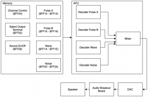
Additionally,  I attempted designing the mixer for the APU. As I was doing this, I learned more about how sound is synthesized. Due to the primitive nature of the Game Boy APU synthesizer, it isn’t clear how the voice information from the decoder is being translated into a wave that can be mixed with other waves. This leads to what I hope to accomplish by the end of next week:

  • Implement and test all the FSMs
  • Finish implementing the datapath for the CPU
  • Understand how to convert decoded information into a wave

Pratyusha’s status report for 02/29/2020

This week, I spent most  of my time understanding the different types of memory on the board, writing the design document, as well as helping with the CPU FSMs. While working on the document, I realized I needed to read more into the SoC and how it integrates with the FPGA and controllers.

I worked on the introduction, memory management, qualitative requirements and SoC sub-system parts of the document.

Since the bios on the SoC has a way of interacting with the USB port (to say, decode NES Controller signals), the next question is figuring out how to get the SoC to talk to the FPGA. We plan on using the SDRAM on the FPGA, using it as MMIO accessible by SOC else, we are going to resort to the FPGA using DDR3 memory on the SOC. I am also looking into the HPS-> FPGA bridge tonight, and will have a more conclusive approach.

Here are the two manuals I am cross referencing at the moment:

Hard Processor System Technical Reference Manual

DE10 Standard User Manual

Meanwhile, SOC has access to the flash memory, can load and store game state.When a game switch happens, the SoC will let the current screen finish rendering and then stop the CPU’s execution. Once the execution is stopped, all of the CPU’s state and the memory will be saved for later re-execution, in flash memory. Afterwards, all of the state will be cleared and the new game state will be loaded in from flash to SDRAM.

By the end of Spring Break, I hope to have:

  • A way of manipulating memory through SoC and FPGA
  • Help with implementing CPU


Tess’ Status Report for 2/29/2020

This week I change my focus and prioritized on working on the design report that is due this weekend. After working on the design review presentation and reading the feedback, we realized there were some details we needed to flesh out before moving forward with implementation. While talking about these details, I was able to get a better understanding of how the APU will interact with the rest of the system. The APU is a purely a read-only sub-system so it will not have any write-backs or interrupt complications like the PPU. This will help with planning and designing interactions amongst the subsystems.

Additionally, from the feedback, we went back and reviewed our verification standard and memory storage. After reviewing the manual again, we realized that we needed a micro SD card to act as our persistent memory because although the board has flash capability, it doesn’t have the storage on the board. Therefore, we have put in a request for a micro SD card so we can begin loading the games and looking at the memory transfer protocols. Additionally, we realized that was no clear “block RAM” on the board so we decided to move our working memory to SDRAM.

For the design document, I wrote the introduction, the APU sub-system description, and the project management.

Before focusing a majority of my time on the design report, I had a chance to start outlining the decoders’ access to memory and wrote out what each bit meant for that voice. By the end of Spring Break, I hope to have:

  • Written out the decoders for the APU
  • Designed how the mixer for the APU
  • Implemented the CPU

Team Status Report 02/29/2020

This week our main focus was the design document because we thought that there was no point in working on implementation when the design is not nailed down yet. This turned out to be a good idea since we discovered some oversights that had been made in our previous plan, we refined our plan for the SoC to FPGA communication as it turned out to be more complicated than we originally thought. We will be using the AXI bus functionality offered by our Cyclone V SoC, which allows us to memory map components of the FPGA to the SoC’s address space. This means that we will have to change our memory solution from block RAM to SDRAM. This shouldn’t be too painful given that the timing guarantees of the SDRAM are still much faster than what we require. We still plan to use block RAM as a stand-in while the SoC sub-system is developed.

Thanks to writing the design document, we now have far more detailed architecture diagrams for our system. As a team, we will start implementing each of the subsystems in the next few weeks. Hopefully, we will be able to have a working prototype by the end of spring break or the week after that. We chose this goal to keep us on track to finish on time and with all of our stretch goals.

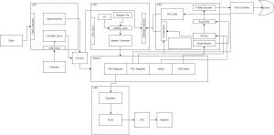
Here is the overall system diagram that we came up with this week: