Tess’ Status Report for 4/26/20

This week we focused on getting ROM0 games to run on the FPGA. This required finding all the small timing and memory bugs that were created by having the memory accesses at a different clock speed. To resolve this, we made our simulation model mimic our hardware model. Additionally, we made as much memory combinational read, meaning an array, to make the transfer easier. Once we were able to get all the synthesis issues and base logic worked out, we got Tetris and Dr. Mario running on hardware!

I spent a majority of the week working on the MBC. I implemented MBC1, MBC3, and MBC5 based on the different documents and reports that people in the community. I worked on debugging through the tests, but towards the end of the week I passed it to Adolfo and started working on the final report and presentation. Due to the refocus, we wanted to make sure we had enough time to implement all the changes. Therefore, I started and lead updating and creating our final report and presentation. Once the presentation is done, I will work with Adolfo to finish getting MBC working on the FPGA.

Goals for next week:

  • Get MBC1, MBC3, and MBC5 working on the FPGA to run more complex games
  • Polish code to match coding standard
  • Finish report

Tess’ Status Report for 4/19/20

This week I worked with Adolfo to get the system onto the FPGA. I was setting up the needed functions on the FPGA through the Megafunction Wizard. We realized that combinational read was not possible using the RAM function so we needed to go back to simulation because our machines can not handle having arrays of that size. So I focused on finding a workaround. Originally we tried using the negative edge of the clock. This worked except in the case where there was a consecutive read and write to the same location. Then we tried giving it a faster clock and that broke our logic. Logically, we knew that the faster clock should work so we looked at the areas that were failing and saw it was a memory to memory transfer, so we adjusted the logic and made small timing changes and we were able to get it to work.

While Adolfo worked on the PPU and the system worked in simulation, the next thing was to support more games. To do this I implemented a memory controller that looked to see which setup the game was expecting. This allowed the games to extend their memory by being able to switch between different ROM and RAM bits. I worked on the controller that currently supports 2 out of the 3 main memory bank configurations. Depending on how these 2 work out, I might be able to get to the third one but that is the rarest of the setups.

Currently, I’m working with Adolfo to get Tetris running in simulation so we can put it on the board. Since our simulation setup matches the one we have on the FPGA, we hope to have everything on the board smoothly.

Goals for next week:

  • Get Tetris, Dr. Mario and a game that uses MBC1 running on the FPGA
  • Polish MBC3 and run a game

Tess’ Status Report 04/12/20

This week I worked with Adolfo to finalize the CPU so we could move towards getting the project onto the FPGA. At the beginning of the week, we had a self-tested CPU that covered a majority of the tasks and we had a working timer and memory. Throughout the week, we realized we had small issues with the memory so we redid that.

We were able to run Blargg’s test suites, one of our benchmark unit test suites. These tests extensively tested our CPU because they tested each possible instruction with every possible bit location and number. Currently, we are able to pass all the tests so we believe we have a solid and completed CPU.

Now we are moving toward putting everything on the FPGA. We have all the components that we need by using the Megafunction Wizard. Currently, I compiling it in Quartus and loaded the memory with one of Blargg’s test so we can test on the board rather than in simulation.

Goals for next week:

  • Able to run Tetris on the FPGA
  • Start working on the memory bank controller to support more games

Tess’ Status Report for 4/5/20

This week I worked on getting the CPU ready for demo and other components to integrate with the CPU. For the CPU, I worked with Adolfo to finish implementing it. This included polishing the ALU and datapath, and implementing miscellaneous instructions. After we implemented all of them, we tested all of the instructions with written unit tests. We wrote the test in asm and Adolfo found a compiler to convert it to a .hex file that the CPU could read. We now have a working CPU that includes interrupts and supports all the instructions.

The next component I worked on was memory. I wrote the memory controller for simulation that would handle memory access from the CPU and PPU. It gives each section in memory its own magic memory. In additional, it handles cases when the PPU and CPU want to write to the same location. In the memory controller, DMA processing are handled, which is when memory in one area needs to be copied to the OAM area. Currently, Adolfo and I are working on implementing the timer so we can run the tim00.gb test from Moonete test suite.

Goals for next week:

  • Implement entire system in simulation
  • Begin system wide test

Tess’ Status Report for 3/29/20

This week I worked with Adolfo on getting the CPU running. I finished coding the datapath with the parts that Adolfo finished coding and worked on polishing the ISA and signals files. To help our testing, I made a magic memory component for our test based on 18341 P6 magic memory.

While Adolfo finished the ALU and decoder, I started writing basic ALU testbenches.  This would make sure our timing was right, the correctness of our output values, and the correctness of our FSM. We plan on creating more unit tests for our components before using the test suite since it will be easier to control the debugging process with our own tests.

Additionally, I worked on writing the updated risk management plan and Gantt chart. I incorporated how we were going to use the unit tests and test suites to minimize debugging integration. The Gantt chart reflects us removing the audio portion, how we changed our division of labor, and schedule changes due to the transition period.

My goals for next week are:

  • Finish debugging the CPU
  • Incorporate interrupts

Tess’ Status Report 03/22/2020

This week we sorted out and finalized what our new project will be due to moving to remote access classes only. We will continue with the original project idea of creating a FPGA Game Boy emulator, but we will no longer support audio due to the lack of access to the lab. We understand that integration will be especially challenging so we will rely even more on the unit test suites and those for the SoC. Additionally, we worked on the SOW to officially refocus the project.

I worked on implementing the datapath for the CPU. A majority of the datapath is coded and hooked up, but I will need to work with Adolfo to assure the signals are correct. Additionally, all of the FSM and signals have been finalized so now we will start integrating the components of the CPU and begin debugging once the decoder is finished.

Additionally, I started looking into “magic memory” that we can use to simulate our CPU before we have memory mapping completed. I looked at 18447 magic memory and 18341 P6. The 18341 P6 will be suffice because it meets our timing requirement and doesn’t require us using segments. To get this to work, we will need to alter the code to work with our CPU and create a .hex file to fake the memory.

My goals for this week:

  • Finish coding the CPU
  • Start testing the CPU with our version of “magic memory”

Tess’ Status Report for 3/14/2020

This week I worked on implementing a majority of the FSMs. After design work, we finally have a framework that we could begin to implement so I started to implement the FSMs based on our datapath. This included setting up the structs that we will need and polishing the timing of certain FSMs.

Additionally,  I attempted designing the mixer for the APU. As I was doing this, I learned more about how sound is synthesized. Due to the primitive nature of the Game Boy APU synthesizer, it isn’t clear how the voice information from the decoder is being translated into a wave that can be mixed with other waves. This leads to what I hope to accomplish by the end of next week:

  • Implement and test all the FSMs
  • Finish implementing the datapath for the CPU
  • Understand how to convert decoded information into a wave

Tess’ Status Report for 2/29/2020

This week I change my focus and prioritized on working on the design report that is due this weekend. After working on the design review presentation and reading the feedback, we realized there were some details we needed to flesh out before moving forward with implementation. While talking about these details, I was able to get a better understanding of how the APU will interact with the rest of the system. The APU is a purely a read-only sub-system so it will not have any write-backs or interrupt complications like the PPU. This will help with planning and designing interactions amongst the subsystems.

Additionally, from the feedback, we went back and reviewed our verification standard and memory storage. After reviewing the manual again, we realized that we needed a micro SD card to act as our persistent memory because although the board has flash capability, it doesn’t have the storage on the board. Therefore, we have put in a request for a micro SD card so we can begin loading the games and looking at the memory transfer protocols. Additionally, we realized that was no clear “block RAM” on the board so we decided to move our working memory to SDRAM.

For the design document, I wrote the introduction, the APU sub-system description, and the project management.

Before focusing a majority of my time on the design report, I had a chance to start outlining the decoders’ access to memory and wrote out what each bit meant for that voice. By the end of Spring Break, I hope to have:

  • Written out the decoders for the APU
  • Designed how the mixer for the APU
  • Implemented the CPU

Tess’ Status Update for 2/22/2020

This week I worked on finishing the FSMs to manage the CPU when there are multi-cycle instructions. Last week, Adolfo and I determined that we would need either one big FSM with multiple branches or multiple smaller ones. We decided to make the smaller ones. I worked on the FSM for the 8-bit ALU operations, 16-bit add operations, pop/push, inc/dec, and CB instructions. Adolfo and Pratyusha are finishing the final 2 FSMs. During this process, I realized there were a lot of flaws in our original CPU datapath so I was updating it with needed connections.

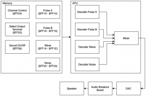
Afterwards, I did more research into how the Game Boy audio works. To save space, the Game Boy had a real time synthesizer because holding an entire audio file in the cartridge took up too much space. There are 4 voices with 5 registers each. Two of the voices are pulse waves that produce the tone. One voice defines the wave shape and the other is used to output white noise. The bits in the register define the voice so each wave needs its own decoder because the bits are in different locations and mean different things depending on which wave you’re looking at. From there, the voices are mixed together and controlled by 3 sound controlling registers. With this information, I was able to design a preliminary datapath for the APU:

With knowing more about the audio, I was able to select and order at DAC. I selected the Monolithic 16-bit AD669 DAC. It is 16-bit with parallel transfer and has a sampling frequency that will be more than suffice for our sound quality. Additionally, it is a through-hole chip, so we need to wire the GPIO pins of the development board to a breadboard. To get the audio into a speaker, we also had to purchase an audio jack breakout board.

Action items for next report:

  • Design how the mixer will work
  • Read through DAC manual to know what circuit requirements are needed
  • Implement FSMs for CPU

Tess’ Status Update for 2/15/2020

This week I worked with the rest of the team to design the datapath for the CPU (which can be found in the team’s status update for the week). Our original CPU design was a two stage pipeline where stage 1 was fetch/decode/execute, and stage 2 was memory. When we learned that all memory accesses use the same memory, we had to rearrange our pipeline. Once done, we were able to add the needed components and connections to match the timing of the Game Boy.

Afterwards, Adolfo and I worked on determining a way to handle multi-cycle instructions. For Game Boy architecture, only 8-bits are sent at a time. Therefore, for multi-cycle instructions, we are continuously receiving new information that is needed for one instruction. To handle this, we decided to use an FSM that would save state for the datapath so it would know which instruction we were handling at all times. The idea is that the FSM will be located in the fetch/decode stage. In the cases of single cycle instruction, it would only enable the pipeline register. In all other cases, it would essentially take the place of the decoder and send the needed control signals. After designing the one large FSM, we realized that it would be cleaner and easier to debug if we had multiple smaller FSMs to handle each category of multi-cycle instructions. We currently have 7 FSMs.

On my audio work, I was researching the different ways we could get audio from the FPGA to a speaker. The first was to use the on-board CODEC that would allow us to directly insert a connection between the board and a speaker. The issue is that the CODEC is dependent on the I2C protocol, which would take significant research, implementation, and testing to assure it is correct on top of the Game Boy audio itself. The alternative is to use a DAC to convert signals for us. This is the more straightforward option because there is no protocol. I have found two DACs that we can potentially use: Monolithic 16-bit DACPORT AD669 and PCM2704CDB. I will continue to look at their data sheets and consult a TA before making a final decision.

Action items for next report:

  • Finish FSMs for CPU
  • Finalize which DAC we will be using
  • Draft an audio datapath