Status Reports

Pratyusha’s status report for 05/03/2020

And we’re done! This week, I worked on building a qsys project for the SDRAM controller from scratch to integrate memory management and attempt game switching on the FPGA.

By the end of the project, for the SoC, we have the controller driver working, SoC and FPGA running simultaneously, as well as the SDRAM (Nios ii) tests working! That comprises the unit tests, and while we got FPGA, SoC to run programs a the same time, we only couldn’t integrate game switching with fpga.

For the rest of the time, I worked with Adolfo and Tess on the final report and demo video, and added my project and code samples to the repo.

You can find SoC code and resources + code with documentation at

https://github.com/tchannn/Game-Boi/tree/SoC

Thanks!!

Adolfo’s Status Report for 4/26

Tess finished the memory bank controllers, which allow us to play more complex games that require more memory.  Meanwhile, I worked on an alternate solution to get the controller to work with the FPGA. I made a controller driver on an RPI and then sent signals to the FPGA through GPIO, with this I was able to play Tetris and Doctor Mario. I also fixed the timer bugs (which means our timer passes all the tests and as a results the sprites in Doctor Mario no longer play at super-fast speed). With this, no bugs were found while playing the games.

Thus, this concludes our main requirements for the FPGA portion of the project. I then restructured the MBC code to work better with the FPGA and then got an MBC1 game working, Super Mario World. This proves that our memory bank controller works in synth as well and that more complex games give our emulator no issues. We’re gonna try to get the off-board memory flashed with games to be able to try out notoriously difficult games to emulate, which require a bit more space than the FPGA has to run. We don’t expect them to work 100% since our PPU isn’t 100% accurate (this is the hardest part to get right in an emulator), but we expect them to be in an otherwise playable state. This is a stretch goal since Tess and I are a bit busy this week so we may not be able to put in as much work as we did in the previous weeks.

We are happy with our results as we have gotten more results than what we had originally aimed for on the FPGA side, even before the COVID issues. Hopefully, we’ll get the external memory on the FPGA to work to do the stretch goal of playing games like Pokemon.

Pratyusha’s status report for 4/26/2020

This week, I worked on integrating the HPS controller code with FPGA program. I created a guide to do the installation and porting over of code to the SoC, and we were able to transfer and run the controller binary on Adolfo’s board, and the controller unit tests worked on his board.

Adolfo and I ran into unforseen problem where we couldn’t flash the FPGA without stopping the program on SoC , or have the program on FPGA keep running while executing the SoC program. We expected the HPS program and the FPGA program to both proceed simultaneously and talk to fpga peripherals.

To fix this, we first tried to get qsys, a system design integration tool, running on Adolfo’s laptop, but due to a bug with Windows/Qsys we couldn’t run Qsys on his laptop. For this temporary hitch, they used an RPI to processor controller inputs while I worked on Qsys.

I managed to integrate the HPS and FPGA parts of the board, with programs running on each of them, through understanding, working with, and writing a program on qsys. Now, we can run a program on SoC while flashing FPGA with a different program.

I also worked on the final presentation and delivery of the same.


Team Status Report for 4/26/20

This week Adolfo and Tess focused on getting ROM0 games running on the FPGA. Together the worked on smoothing out the final timing and memory bugs that came up when implementing the work around for combinational read on the FPGA. Once Tetris start running, Tess focused on debugging MBC1 and MBC3. Adolfo worked on fixing the small PPU bug that became apparent when running Dr. Mario.

Once Dr. Mario was running, Adolfo took over debugging the MBCs and Tess start updating and creating the final report and final presentation. Adolfo debugged the MBC by creating a small FSM to support the boot rom process, and allowing memory to dynamically adjust the different cartridge and ROM size. He was able to get it working in simulation, but there is still an issue with MBC on the board. Adolfo and Tess will investigate this once the presentation is over.

Additionally, while Adolfo was working on getting larger games onto the board, our on chip memory isn’t big enough to run games larger than 512 kB. To work around this, Professor Nace has given a new board so once we figure out the MBC bug we will move to the new board to try larger games.

Pratyusha and Adolfo setup the SoC on Adolfo’s board, and we were able to transfer and run the controller binary on Adolfo’s board, with controller unit tests passing. They ran into unforseen problem where they couldn’t flash the FPGA without stopping the program on SoC , and couldn’t have the program on FPGA keep running while executing the SoC program. We expected the HPS program and the FPGA program to both proceed simultaneously and talk to fpga peripherals.

To fix this, we first tried to get qsys, a system design integration tool, running on Adolfo’s laptop, but due to a bug with Windows/Qsys we couldn’t run Qsys on his laptop. For this temporary hitch, Adolfo used an RPI to processor controller inputs while Pratyusha worked on Qsys. Now, she can run a program on SoC while flashing FPGA with a different program.

As a team, we will work on finishing the presentation this weekend and preparing for the presentation on Monday. Once the presentation is over, we will focus on finishing the report. Adolfo and Tess will also focus on determining the MBC bug, and then polishing the code and repo.

Tess’ Status Report for 4/26/20

This week we focused on getting ROM0 games to run on the FPGA. This required finding all the small timing and memory bugs that were created by having the memory accesses at a different clock speed. To resolve this, we made our simulation model mimic our hardware model. Additionally, we made as much memory combinational read, meaning an array, to make the transfer easier. Once we were able to get all the synthesis issues and base logic worked out, we got Tetris and Dr. Mario running on hardware!

I spent a majority of the week working on the MBC. I implemented MBC1, MBC3, and MBC5 based on the different documents and reports that people in the community. I worked on debugging through the tests, but towards the end of the week I passed it to Adolfo and started working on the final report and presentation. Due to the refocus, we wanted to make sure we had enough time to implement all the changes. Therefore, I started and lead updating and creating our final report and presentation. Once the presentation is done, I will work with Adolfo to finish getting MBC working on the FPGA.

Goals for next week:

  • Get MBC1, MBC3, and MBC5 working on the FPGA to run more complex games
  • Polish code to match coding standard
  • Finish report

Adolfo’s Status Report for 4/19

This week I focused on getting the PPU finished and in an “excellent” state. I did this by running the dmg-acid2 test, which helped us pinpoint all the inaccuracies that the PPU had.  I spent a good chunk of the week getting it running, as I was confident that with this test and our CPU verification tests we would be good to run most games that we throw at the emulator.

Furthermore, after much struggle, Tess and I managed to get the core running on the FPGA. We were able to run some tests, but there were some glaring graphical glitches. This was because we had not accounted for the memory not having combinational reads, all the memories offered by the FPGA required registered inputs. We got around this by speeding up the clock and changing some internal details to account for this change. In the end, it worked out!

Furthermore, I planned out the joypad integration into the Gameboi. I read the docs and made a module where we can just plug in the controller’s signals to make it work.

After getting the FPGA working with the whole system, we were able to run the PPU stress test on the board and all the other instruction tests we ran before, with the same results as simulation. I am excited to say that we also got Tetris and Doctor Mario running. Tetris didn’t seem to have any bugs and Doctor Mario was suffering from some timer issues, which I think we have diagnosed.

This week we’ll get memory banking working so that we can run all of our stretch goal games. Furthermore, we’ll also squash any bugs that remain. Our goal is to have the Gameboy working without game switching by the end of the week. We are also looking into an audio module that looks promising, it is built for our FPGA so it’s worth a shot!

Pratyusha’s Status Report for 4/19/20

This week I had two objectives

  1. To get the USB Controller driver working
  2. To get the SDRAM NIOS test running on the board

For 1. as per last week’s meeting, the last approach I was going to attempt before switching over to USB/ps2 keyboards was to checkout into the linux kernel version of the angstrom distribution, specifically to the unofficial commit of the drivers, compile the module with the linux source tree of that version, figure out the special flags needed for compilation, and then port over that driver to the board, load it without conflict to existing linux code and drivers, and then attempt to identify the controller through the driver.

There was an initial conflict with compiling both joypad and hid-dr modules, but after realizing that we could make do with just hid-dr, I chose to stick with that, and it ran with the existing linux source code, and I was able to retrieve bytes form the controller.

To make the NES-controller….controller, I had to understand the event structures, types and linux/input.h, details linked here. I then composed code to handle multiple presses and releases of the controller inputs, where the button packets were of different lengths, so I implemented a variable length buffer to handle this.

All in all, the end result is as shown here. Each button press and release maps to the respective led being on and off.

2. The next goal was to get qsys running on the VM, and compile a basic program. The manual also had an example of an SDRAM test, with installation setups, unique to Windows, so after finding workarounds for the linux VM, I got the SDRAM NIOS2 test to work on the FPGA board. This means we can copy over information to the SDRAM from the SoC, and read back from it and compare the bytes, to check if they are the same. Still have to implement checking the sums being equal for the bytes on FPGA and SoC.

Thus, this weeks goals were achieved. The goal for this week is to read from USB storage, and write those bytes to SDRAM, read them back and store it on the USB flash. I expect working with Qsys to be non-trivial for the same :'(.  Using USB instead of micro SD card because currently the board boots from the micro SD card and I don’t want to mess with it.


Tess’ Status Report for 4/19/20

This week I worked with Adolfo to get the system onto the FPGA. I was setting up the needed functions on the FPGA through the Megafunction Wizard. We realized that combinational read was not possible using the RAM function so we needed to go back to simulation because our machines can not handle having arrays of that size. So I focused on finding a workaround. Originally we tried using the negative edge of the clock. This worked except in the case where there was a consecutive read and write to the same location. Then we tried giving it a faster clock and that broke our logic. Logically, we knew that the faster clock should work so we looked at the areas that were failing and saw it was a memory to memory transfer, so we adjusted the logic and made small timing changes and we were able to get it to work.

While Adolfo worked on the PPU and the system worked in simulation, the next thing was to support more games. To do this I implemented a memory controller that looked to see which setup the game was expecting. This allowed the games to extend their memory by being able to switch between different ROM and RAM bits. I worked on the controller that currently supports 2 out of the 3 main memory bank configurations. Depending on how these 2 work out, I might be able to get to the third one but that is the rarest of the setups.

Currently, I’m working with Adolfo to get Tetris running in simulation so we can put it on the board. Since our simulation setup matches the one we have on the FPGA, we hope to have everything on the board smoothly.

Goals for next week:

  • Get Tetris, Dr. Mario and a game that uses MBC1 running on the FPGA
  • Polish MBC3 and run a game

Team Status Report for 4/19/20

This week the goal was to set up everything for integration. Adolfo and Tess started moving the simulation CPU onto the FPGA. Unfortunately, they thought that combinational read memory would be available. Tess focused on finding a work around and updating the logic to match. She was able to solve this issue by using a faster clock for memory. Since synthesis takes a long time for such a large project, she updated the simulation model to match what the FPGA would look like.

Since the CPU is essentially done for games that only use ROM0, Tess moved onto implementing a memory bank controller (MBC) so the emulator could support more games. This required creating a controller that controlled memory accesses to a different memory location so the CPU was hidden from the difference.

Adolfo focused on finishing and then perfecting the PPU. Since last week, he polished implementing scroll and fully implemented and tested sprites. Although the PPU was already passing more tests than other emulators, but his goal was to pass almost all of them to clearly pass our expectations. He had to refine his logic because of the timing and memory change, but then he worked on perfecting the display. He is debugging a test that displays a face because it is a hard test that specifically targets all the small details of the PPU.

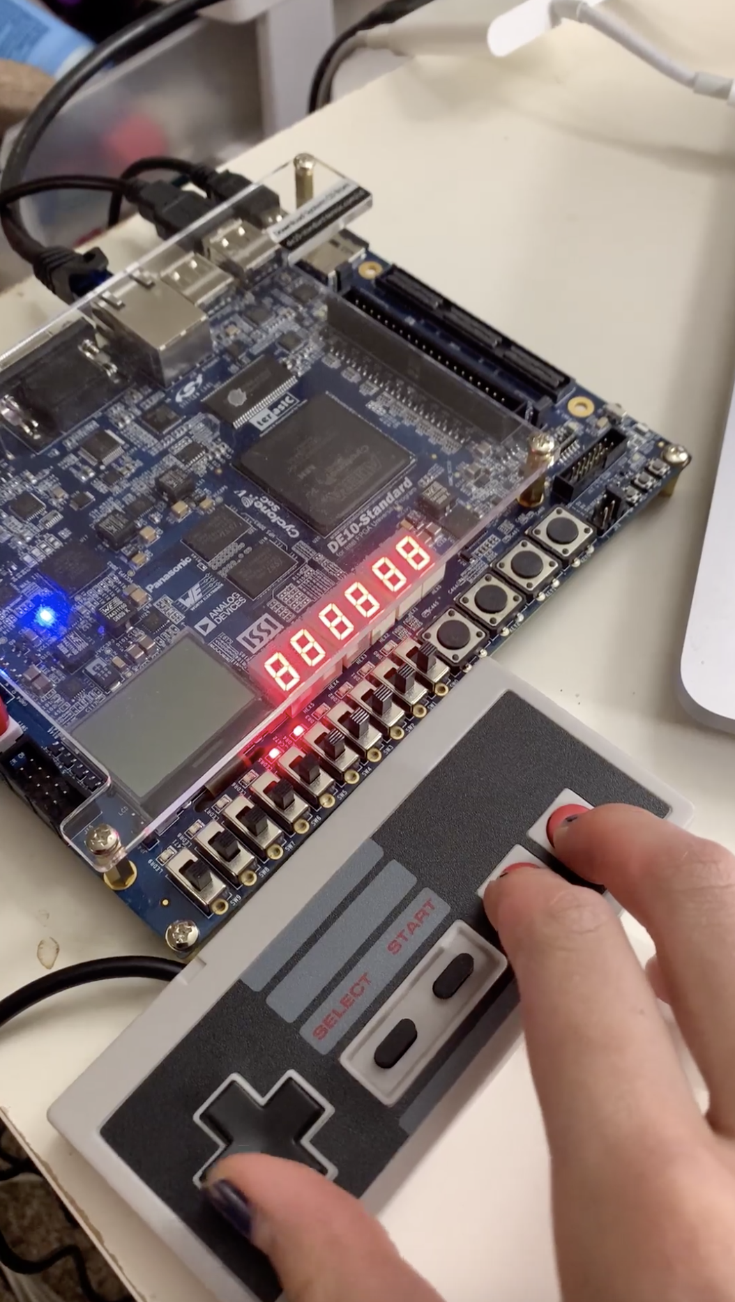
Additionally, Adolfo set up the registers on the FPGA side to accept joypad inputs. He is now working with Pratyusha to get the SoC to write to those registers.

By tomorrow’s demo, they hope to have Tetris running on the FPGA.

This week, Pratyusha  had two objectives –

  1. To get the USB Controller driver working
  2. To get the SDRAM Nios-2 test running on the board

For 1. Pratyusha compiled modules with an unofficial version of the linux kernel with special flags, and ported over drivers to the board, which after configuration could receive bytes from the controller. For the NES-controller’s controller, she understood the event structures, types and linux/input.h, details linked here, and then composed code to handle multiple presses and releases of the controller inputs, and dealt with variable length packets.

All in all, the end result is as shown here. Each button press and release maps to the respective led being on and off.

2. Additionally, Pratyusha got the SDRAM NIOS-2 test to work on the FPGA board. This means we can copy over information to the SDRAM from the SoC, and read back from it and compare the bytes, to check if they are the same. Still have to implement checking the sums being equal for the bytes on FPGA and SoC.

Goal for this week is to read from USB storage, and write those bytes to SDRAM, read them back and store it on the USB flash.