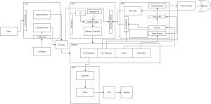
This week our main focus was the design document because we thought that there was no point in working on implementation when the design is not nailed down yet. This turned out to be a good idea since we discovered some oversights that had been made in our previous plan, we refined our plan for the SoC to FPGA communication as it turned out to be more complicated than we originally thought. We will be using the AXI bus functionality offered by our Cyclone V SoC, which allows us to memory map components of the FPGA to the SoC’s address space. This means that we will have to change our memory solution from block RAM to SDRAM. This shouldn’t be too painful given that the timing guarantees of the SDRAM are still much faster than what we require. We still plan to use block RAM as a stand-in while the SoC sub-system is developed.
Thanks to writing the design document, we now have far more detailed architecture diagrams for our system. As a team, we will start implementing each of the subsystems in the next few weeks. Hopefully, we will be able to have a working prototype by the end of spring break or the week after that. We chose this goal to keep us on track to finish on time and with all of our stretch goals.
Here is the overall system diagram that we came up with this week: