Roshan Nair – Weekly Status Report #5

This week has been primarily focused on efforts to get the mvp working. Therefore I have been continuing on with the adc and dac modules and verifying them. Additionally through discussion with my team members we came up with a plan for what the top level MVP module should look like. What we need initially for testing is just the ADC, DAC, and then a simple register to latch the audio values between them (no processing). This will be useful just to debug all the points of the system. From there we can move on with including panning and bit crushing in the pipeline for MVP effects.

This is an example of the ADC clock dividing by 8, the data lines getting latched in, and the word select line toggling after the 32 bits.

Team A0 – Weekly Status Report #5

This week we are mainly in preparation mode as the integration part of our project nears and we need to get ready for the MVP demo.

Roshan has been working on the ADC and DAC handlers on the fpga side since the ICs we’ve used utilize a serial bus to send the digital data. He has also continued looking into effects for our MVP.

Nick P has assembled the PCB and done some basic testing aswell as continuing to research FFT implementation options as this is a critical part for some of our more complicated effects.

Nick S has been working on the MIDI decoding module, which has involved testing through the use of testbenches for various sub-elements of the module as well as debugging.

We seem to be on track for a successful MVP by the first demo date.

Nick Saizan – Weekly Status Report #5

This week I was very busy finishing up a lab, but I found the time to help Nick P our a little bit with reflowing our PCB, and the majority of my time on this project was spent debugging/testing the Midi Decoding Verilog code. There are still some timing issues which need to be worked out as we begin to integrate, but it seems to be working decently so far. Attached is a screenshot of the testbench output for the module. The compression is pretty harsh, however you’d be able to see a new pitch/velocity pair show up in the arrays as the data is received over a simulated midi interface.

Nick Paiva – Weekly Status Report #5

This week, one of the things I’ve worked on is assembling the PCB for our project. We then connected the FPGA to power, and everything seems to be working correctly so far. We were able to see MIDI coming into the board on the oscilloscope. Here is a picture of the board while powered on:

I’ve also looked into the FFT further. As it turns out, there is an IP core FFT for the Cyclone V. It seems as though it would work well for our purposes, and would make the implementation process much easier. It seems that we would still have to manage the memory that this IP uses, but that we can easily just pass in samples in natural order.

Finally, I also looked into the display driver more. The display uses a SPI-like interface, and takes data in one bit at a time. It should be relatively easy to write a driver that can send out data in the required format. The harder part is going to be embedding a state machine in hardware that sends all of the required commands to the display. The documentation for the display is not the best, so it is unclear exactly what commands need to be sent to write to pixels on the display. The datasheet for the on board driver chip may be more useful in that regard.

Nick Saizan – Weekly Status Report #4

This week I worked on the MIDI Decoding part of our project. My first steps were to being looking at the waveforms of our MIDI keyboard and begin to inspect the actual data it was sending. My goal was to confirm that the information is was sending is consistent with the research I’ve done so far on the MIDI interface.

The above picture is the waveforms generated from both a KEY-ON and a KEY-OFF message. On the left side you can see that one of the bits in the first byte is different. this is consistent with 0x90 for KEY-ON and 0x80 for KEY-OFF, which is a part of the MIDI standard. One of the challenges was realizing that each byte is sent in reverse bit order, and there is a low bit to signal the start as well as a high bit to signal the end of a byte. While the inner byte order is reversed the ordering of byte amongst each other is not.

With this information I was able to begin working on the MIDI Decoding FSM/Datapath. Currently the only messages we care about are NOTE-ON, NOTE-OFF, and AFTERTOUCH. And thus that is why those are the only types of commands read by the FSM. Writing the whole MIDI decoding system out was a little over 300 lines of systemverilog, however I have not had the chance to test it.

Team A0 – Weekly Status Report #4

Now that the PCB is ordered, this week was focusing on integration in order to get audio working through the fpga. Therefore the ADC and DAC modules are a priority as well as getting communication from the MIDI device through the MDI decoder.

Roshan is bringing up the ADC and DAC.

Nick S is bringing up the MIDI Decoder (we measured the keyboard outputs and it follows the protocol as expected).

Nick P is focusing on doing more research for FFT and efficient ways to store samples as a lot complicated effects require these.

Roshan Nair – Weekly Status Report #4

This week was continuing to test the panning and bit crushing modules in simulation as well as in the python model. Additionally development/testing for the adc module is ongoing and development for the dac module.

The gathered specs for the adc model are listed below:

ADC Translator
Master clock = 25 MHz
B Clock = 32 clocks for left, 32 clocks for right (3.125 MHz)
Word Select = left channel (0) right channel (1)
Dout = comes left channel (MSB – LSB) and right channel (MSB – LSB)

So I have been working on changing this spec to actual rtl. The rtl consists of an audio buffer that is 32 bits wide (2 channels). Out of these 32 bits only 24 are valid and from those 24 we are only using 16 bits for our DSP. After every two audio frames (2 channels) then a valid is asserted for the next DSP block to latch the audio data. From here a new buffer starts to be created with the new audio values. Additionally the B clock is 25 Mhz divided by 8 which is implemented with a simple counter.

On another note in simulation we started to hear what sample audio sounds like in 8 bit mode. The result seems to be very noisy with the current example because those 8 bits seemed to have carried a lot of the audio info. Looking online we may need to normalize the audio to make this a useful effect.

Nick Paiva – Weekly Status Report #4

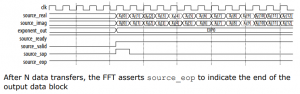
This week I have looked into how we would implement frequency filtering and pitch shifting. I’ve been reading through this document on an FPGA implementation of the FFT to get an idea of how we would implement this in hardware. Additionally, I’ve been reading up on signal processing theory to get an idea of how we can make this block both efficient and high-quality (low latency, preserves low frequencies).

What I’ve found is that there is a fundamental trade-off between the latency that we introduce into our pipeline and the lowest frequency that we can preserve in our signal. The lower the frequency, the larger the delay. This follows from the idea of Rayleigh Frequency. We need to collect enough points to properly represent a low frequency, and collecting those points introduces delay.

To minimize delay through the pipeline but still preserve the lower frequencies, we should use a window size of 512 points. The total delay through the pipeline would be ~20ms, and we would be able to capture frequencies as low as 94 Hz. Here are some of my notes for this calculation:

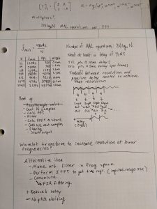
Alternatively, we can solve filtering and pitch shifting in the time domain. For filtering, we could implement an arbitrary digital filter in the frequency domain and then use the IFFT to find its impulse response. Then, it would be a simple matter of implementing a convolution with a FIR (Finite Impulse Response) filter. This method should introduce a smaller amount of delay for the same frequency resolution. For pitch shifting, we could use the Shift OverLap and Add method (SOLA).

The final implementation of this effect will warrant a larger discussion about desired tradeoffs.

Roshan Nair – Weekly Status Report #3

I didn’t get as much done this week due to an onsite interview taking a large chunk of the week. However I continued testing the panning module and starting setting up a more concrete testbench that we can extend for the more complicated blocks. Essentially it consists of comparing python wav dumps with the equivalent SV wav dumps. Additionally I started implementing the verilog for the bit crushing module which zeros out the 8 LSBs.

For more of top level perspective I also been on the side stripping away the SDRAM IP block down to a simpler level just so its easier to integrate. Additionally I continued to help the team to make concrete protocols between each of these blocks for integration.

Team A0 – Weekly Status Report

We’ve all been busy with job fair stuff so we haven’t gotten too much done this particular week. We have been looking into implementing different effects and drivers, and plan on writing more Verilog and ordering parts for the PCB this week. We hope to have some basic representations of some effects by the end of the week, and detailed plans for others. In class discussions we also clarified the different clock domains and discussed how much performance leeway we have in terms of latency of each dsp block.