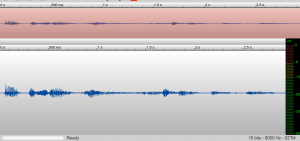
Since this is the last week before the public demo it has mostly been about wrapping up on effects and cleaning any minor bugs so far. Delay/Echoing is complete with a variable delay however it seems to clip very briefly when changing from a short delay to a very large delay for some reason. I am still looking into fixing that. Additionally the goal is to also add Reverb which I am currently working on now. These will require the addition logic to the memory controller to arbitrate between requests since it is shared between modules.
Author: rsnair
Roshan Nair – Weekly Status Update #8
This week was finalizing some of the bugs faced with bit crushing and panning with MIDI. Additionally I have started the verilog and microarchitecture for echoing which is currently being tested in simulation but will soon tried on the FPGA using the SDRAM chip. The MIDI keyboard will be able to dynamically change the delay of the echo based on the pressure.
Additionally I helped Nick P. briefly for debugging the display controller.
Team A0 – Weekly Status Report #7
Since we were able to get audio passthrough working, we each of have been continuing on the other aspects of the project.
Nick P. has been working on researching how to implement FFT in verilog for the complicated effects that need the frequencies of a window of audio. Additionally he has been looking into the screen display protocol since it may be useful for real time hardware debugging.
Nick S. has been working on getting the MIDI FSM decoder to work in hardware. This has been a combination of testing in simulation as well as testing in the board to make sure the essential key presses and velocity changes are working as intended.
Roshan has been working setting up the pipeline for all the audio effects. This includes the now working ADC/DAC modules, the synchronizing registers between the slower and faster clock domains, and the instantiation of the effect modules in the proper order.
Roshan Nair – Weekly Status Report #7
This week I have been working on implementing the micro architecture for the effects pipeline.
Since last week we were able to get audio pass through working by hooking up the adc data line to the dac data line within the fpga…this week we actually tested the shifting registers in verilog itself with the dac and adc interfaces. Initially we got extremely noisy audio. However I was able to fix the issue by changing the dac driver to be negedge instead of positive edge since the dac chip samples it on the positive edge.
Additionally instead of doing the native 24 bit audio we changed to 16 bit as defined by our spec and it seems to still have clean audio. Now I am working on setting up the synchronization registers for transferring the audio between clock domains (3.125 Mhz for dac/adc and 50 Mhz for effect processing).
Roshan Nair – Weekly Status Report #6
This week was primarily towards getting audio pass through working for the demo next week. Along with the general debugging that all of us had to do, I was in charge of setting up the basic verilog to drive the necessary clocks and pass the adc output to the dac.
To summarize: System Clock (25 Mhz), B Clock (3.125 Mhz), Word Clock (48.8 Khz)
Each of these were driven to the corresponding GPIO pins on the FPGA to properly control and configure the IC chips.
There were initial problems of the values not driving on the correct pins but this was due to the indexing bits in verilog being different than the actual physical pin.
Roshan Nair – Weekly Status Report #5
This week has been primarily focused on efforts to get the mvp working. Therefore I have been continuing on with the adc and dac modules and verifying them. Additionally through discussion with my team members we came up with a plan for what the top level MVP module should look like. What we need initially for testing is just the ADC, DAC, and then a simple register to latch the audio values between them (no processing). This will be useful just to debug all the points of the system. From there we can move on with including panning and bit crushing in the pipeline for MVP effects.
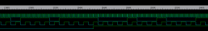
This is an example of the ADC clock dividing by 8, the data lines getting latched in, and the word select line toggling after the 32 bits.
Team A0 – Weekly Status Report #4
Now that the PCB is ordered, this week was focusing on integration in order to get audio working through the fpga. Therefore the ADC and DAC modules are a priority as well as getting communication from the MIDI device through the MDI decoder.
Roshan is bringing up the ADC and DAC.
Nick S is bringing up the MIDI Decoder (we measured the keyboard outputs and it follows the protocol as expected).
Nick P is focusing on doing more research for FFT and efficient ways to store samples as a lot complicated effects require these.
Roshan Nair – Weekly Status Report #4
This week was continuing to test the panning and bit crushing modules in simulation as well as in the python model. Additionally development/testing for the adc module is ongoing and development for the dac module.
The gathered specs for the adc model are listed below:
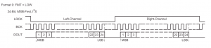
ADC Translator
Master clock = 25 MHz
B Clock = 32 clocks for left, 32 clocks for right (3.125 MHz)
Word Select = left channel (0) right channel (1)
Dout = comes left channel (MSB – LSB) and right channel (MSB – LSB)
So I have been working on changing this spec to actual rtl. The rtl consists of an audio buffer that is 32 bits wide (2 channels). Out of these 32 bits only 24 are valid and from those 24 we are only using 16 bits for our DSP. After every two audio frames (2 channels) then a valid is asserted for the next DSP block to latch the audio data. From here a new buffer starts to be created with the new audio values. Additionally the B clock is 25 Mhz divided by 8 which is implemented with a simple counter.
On another note in simulation we started to hear what sample audio sounds like in 8 bit mode. The result seems to be very noisy with the current example because those 8 bits seemed to have carried a lot of the audio info. Looking online we may need to normalize the audio to make this a useful effect.
Roshan Nair – Weekly Status Report #3
I didn’t get as much done this week due to an onsite interview taking a large chunk of the week. However I continued testing the panning module and starting setting up a more concrete testbench that we can extend for the more complicated blocks. Essentially it consists of comparing python wav dumps with the equivalent SV wav dumps. Additionally I started implementing the verilog for the bit crushing module which zeros out the 8 LSBs.
For more of top level perspective I also been on the side stripping away the SDRAM IP block down to a simpler level just so its easier to integrate. Additionally I continued to help the team to make concrete protocols between each of these blocks for integration.
Roshan Nair – Weekly Status Report #2
This week was continuing to come up with a concrete plan for how to structure the verilog code base.
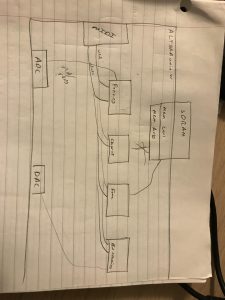
This was just a rough sketch done in lab, but through the discussion we organized all of the major modules required for the integration phase.
The panning module was written and I started testing and verifying the module. Based on a discussion with the rest of the team and Professor Nace we realized that having some sort of testbench that can use example wav files for the generated data and sending it through the DSP modules will be an efficient way of testing. At the same time we can ensure that our algorithms are correct from a auditory perspective by playing back these wav files and making sure that the sound played is the effect we expected.
This is an example wav file that I have been using for testing purposes. I have written python code that allows us to read the data (stereo) by each audio frame. The plan is to then dump these values into some sort of systemverilog array file so that we can instantiate a driver to read and drive these values into our module for testing purposes.