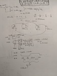
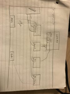
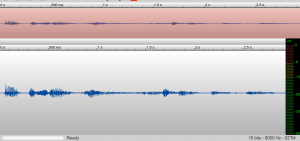
This week my two goals were planning the chorus effect, and getting familiar with the MIDI output of the keyboard. For the chorus effect I had many things to consider. For example, I first needed to know how much memory I would need for an effect like this. So by taking our 44.1kHz sampling rate, 2-channel, 16 bits per channel audio, I was able to calculate that we’d need about 176kB of memory per second of audio we wanted to store. Based on qualitative tests in Audible where I tested various delays, I found that about 0.025s of delay between copies of an audio signal was where the effect started to sound unpleasant. So as a result I used this value to calculate that 4.410kB of storage was necessary for this effect. After discussion with the rest of the team we believe that using the onboard block ram of the fpga was the best solution, because we wanted to ensure our SRAM didn’t have other effects that might interrupt echoing’s performance. I’ve been looking into how to infer block ram in SystemVerilog code as well. My plan for the chorus effect is to constantly store the audio stream in my allocated block ram space, and then pull out copies at varying intervals from the stored data, depending on how much delay I want and how many “voices” I want in the effect. I also spent some time cleaning up our top level SystemVerilog module. This involved adding comments and headers for code readability as well as setting up a rough structure for how our effects will be integrated into and enabled within the top level module. The last thing I did this week was start to get a sense of how our MIDI keyboard is actually sending data, and begin to correlate that with the research I’ve done on the MIDI protocol. I’ve attached images of some of the signals I’ve seen. There is a MIDI start command and end command as well as some other data bytes related to the aftertouch capability. start status byte
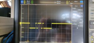 data byte
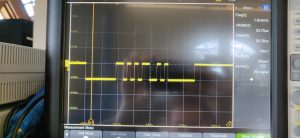 end status byte
This week we appear to be on schedule as the keyboard was shipped very quickly with amazon prime so I was able to begin testing already. Next week I hope to implement a MIDI decoder module in the fpga.