This week, I have worked on finalizing the PCB design. Since last week, I’ve added some extra components, double checked connections, and refined the layout. Here is the finalized schematic design: 
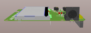
The final PCB is designed to slot into the GPIO connectors and replace the acrylic face plate on top of the FPGA. Here are renders from the top and side views respectively:

I have also completed a BOM for the PCB. For a single PCB, the BOM cost will be about $45. Here is a screenshot of the BOM:
