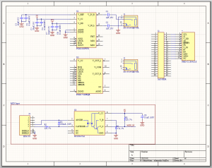
This week I worked on component selection and the PCB schematic design. As part of this I have worked on both schematic and layout symbols for all of the major parts. Now that I have most of the major symbols done, it will not take much longer to finish the schematic and get the PCB layout done.
In progress schematic:
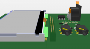
3D CAD view:
For next week, I hope to have the PCB design finished.