Mihail’s Status Report for 04/25

This week I gave the final design presentation for my team, continued debugging efforts for the filter before pivoting to a new approach, integrated the LCD display into our system, and continued testing.

The start of my week was spent preparing the slides for the final presentation, and then I spent substantial effort Sunday, Monday, and Tuesday practicing it.

I spent more time trying to debug the filters in parallel to this but was unable to find the underlying bug. I’ve decided I’ll have another teammate look at the issue, but instead of allowing this to block progress, I decided to work around the problem and implement a “pseudo-filter”. The module looks at the primary frequency being played and uses that to attenuate the inbound data, and takes in cutoff frequencies and gradients as inputs. I’ve designed it so that it can operate as a  low, high, or bandpass filter depending on user inputs, with independent cutoffs and gradients on each end. Users will be able to program the filter type via the UI.

With the workaround implemented, I wanted to focus on system integration. I selected a LCD display to be added to the system and programmed it. This was slightly difficult since the graphics system was different from what I was used to (X and Y coordinates were flipped and pixel coordinates did not start in the top-left corner as is standard). I managed to implement functions that allow me to display arbitrary strings on the display, and added code to our Arduino to initialize and display messages on the LCD code as well as interface between the MIDI and FPGA. After adding debouncing logic to avoid rewriting values every single time a knob was turned (instead, only after a set amount of time had passed), I had the LCD display input parameters. As of now, this is ADSR inputs. Once the system is fully integrated, I will have it display the different values for whatever the filter selection input is currently on.  We’ll still have the VGA output provide visual cues for what certain effects are doing, while the LCD display is designed to give numerical data.

Finally, I spent some time testing, specifically working on testing setup times, something that is still possible despite the UI not being fully integrated. I’m also preparing for another round of SQNR tests to ensure that the sawtooth and square waves are now at acceptable values.

Next week, I will finish integrating the system, perform more tests as necessary, make one last pass at the original filter implementation, and give our design expo as well as write the final design report.

Mihail’s Status Report for 04/18

I spent the week working preparing for the final design presentation, which I will be giving, and trying to debug the low pass and high pass filters now that I could do so on board.

For the first task, I spent time working preparing the slide deck and practicing it, as well as gathering testing data with my partner, Jose. We determined it would be wisest to use different testing metrics than the ones we had originally intended, choosing to focus on latency, audio quality, and audio accuracy due to their ease of testing and higher relevance relative to our original metrics. From there, the components for MIDI processing were setup as a separate circuit and tested with an oscilloscope, while the on board components were tested by inserting cycle counts into the FPGA to determine the amount of time between an input signal being registered and a change in the output audio.

Debugging the filters has proven to be a large time sync, since I am still not achieving the results I had desired for (with the filters tending to either not filter at all, or filter too aggressively for coefficients that should still pass through a variety of the notes on board). As a result, I spent some time creating a python script that would simulate the fixed point arithmetic of the filters and compare that a golden model using floating point. Below included is the expected attenuation for the low pass filter I’ve chosen as the best candidate for final inclusion, a 5 stage, cascaded, first order filter. At this point, I am fairly convinced that the issue is with how I am dealing with sign logic, or due to some unexpected way in which the compiler is translating my RTL. I hope to have resolved the issue by the end of next week, but will be spending a large amount of time on system integration.

During this course, I’ve found that I’ve gained a lot of knowledge in how to simulate digital logic, learning both MATLAB (for the second time) and python’s numpy / scipy libraries in order to develop, test, and debug components. Additionally, I learned a lot on how to use Quartus, since my experience had primarily been in guided tutorials before, and I now feel that I have a much better understanding of the tool. For these, I’ve found that there tend to be a variety of resources online that I can use a start base for my knowledge, and found generative AI very useful to help me plug gaps in my knowledge (i.e. asking for clarifications regarding a paragraph in a article I read). From there, moving on to more technical articles such as the official documentation for a library or software allowed me to gain the knowledge I needed.

Mihail’s Status Report for 04/04

Unfortunately a large part of my week was spent dealing with a Quartus issue; for some reason, I lost the ability to program the FPGA itself, and had to invest a large amount of time finding a workaround. As a result, I focused my effort on setting up a testing pipeline in simulation in order to look at filter / delay outputs and ensuring their stability. Once I got that to work, I debugged delay, and it looks like it works without having to clamp the delay feedback coefficient. Additionally, I used the IIR components to construct a single-pole and biquad low pass filters, and created a cascade filter using multiple single-pole IIR filters. I seem to have finally resolved the Quartus issue today, so I hope to spend tomorrow verifying the filters on the FPGA and qualitatively comparing their outputs, and to spend a large portion of next week ensuring that FM is working properly.

In terms of system testing, I hope to use the pipeline I’ve already set up for the delay output. Primarily, the testbench I’ve designed allows me to optionally add in parts of the pipeline (such as FM, ADSR, delay, etc.), and check how components interact with one another and gather data on output waveform. From this, basic visual inspection can help ensure output stability and that the output is approximately what would be expected. Checking the collected data against MATLAB scripts can allow for further verification, especially on components like a low-pass filter, where the expected output is not immediately obvious. A final check can be performed on the actual FPGA, something I am able to do now that Quartus has been configured properly. Since delay, FIR, and IIR filtering all go in the portion of the pipeline, the testing process is exactly as described above – configure the audio pipeline so we can isolate the specific component in simulation, and then perform progress checks on the output. For FM modulation, the process is slightly different, namely that I intend to directly compare against MATLAB scripts, rather than trying to visually determine if the waveform “looks” correct. I intend to remove all downstream portions of the audio processing pipeline, looking directly as how the wavetable index / waveform output behave.

Team Status Report for 03/28

This week, we focused on preparing for the interrim demo and planning out interface for the final design. We feel that most of the components are coming along well and we hope that we will have time to add in additional features and a nicer interface using an Arduino with knobs / buttons. The schedule has not changed and we feel that we are in a good spot, our major risks going forward are with filtering and the MIDI breakout board being more complicated than expected. Nonetheless, we have ended the week feeling optimistic and fairly prepared for the upcoming demo.

Mihail’s Status Report for 03/28

I spent most of this week with my teammates preparing for the upcoming interrim demo. For the first half, I realized that there was a core issue with how I was implementing frequency modulation earlier and decided to redo it based off of articles I found online, mainly, I now use two oscillators. The first is the baseline that is already used to perform wave table lookup, and the second oscillator is used to modulate the first. I am still in the process of debugging this and do not believe it will be done before the demo, but I plan on running simulations and comparing outputs to matlab scripts – one of the standard testing processes as described in our design report.

The second half of the week was spent on adding delay to the actual FPGA and debugging. The delay module was added into the pipeline after ADSR. A major bug was output amplification, it turned out that I was incrementing the feedback gain too rapidly. This seemed to cause the output amplitude to rapidly reach its maximum, causing a very unpleasant noise to constantly be emitted from the FPGA. I am still trying to understand the source of the issue, but clamping the value of the feedback coefficient g was enough to resolve it. I still plan to spend tomorrow gathering data in order to better understand the cause of the issue, so that I can avoid it for other filters. I intend to spend next week further debugging FM, and hopefully beginning to add in FIR and IIR filters.

Mihail’s Status Report for 03/21

I spent most of the week debugging the RTL for the FIR filter component, and implementing infinite impulse response (IIR) filtering. The primary difference between FIR and IIR filtering was that IIR filtering also considers past output values as well as prior inputs, increasing the number of weights that needed to be stored as well as the number of steps in the adder tree. I decided that it was simpler to maintain prior values for both X[n] and Y[n] as shift registers, rather that storing them in BRAM, since, based off of my research, IIR filters do not need to store a large amount of terms. The bookkeeping circuitry eliminated by moving to a sliding window approach seems to outweigh using registers instead of BRAM to store prior input / output wave data. With audio output configured correctly, I also looked into verification. I began writing testing scripts in MATLAB to generate “golden models” for various filters / on board components, mainly looking at the Signal Processing Toolbox. The main question remaining is how to properly capture output from the FPGA synthesizer itself, a problem which I hope to solve in the following week so that we can perform some validation / refinement before the interim demo.

Mihail’s Status Report for 03/14

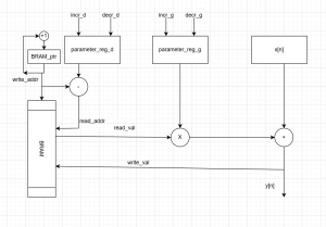
A substantial portion of my time this week was spent on the personal portion of the ethics assignment. With my remaining time, I began implementing the FIR filter component. To design the filter, I parameterized the RTL so that an arbitrary number of prior samples x[n−i] could be stored in on-board BRAM. I then used the param_registers, modules I created last week to store the filter coefficients b_i. The combinational logic reads each stored sample x[n−i] along with its corresponding coefficient bi, and multiplies the pair using a DSP slice. This approach is similar to the one used in the delay component; I found that the design effort saved by leveraging DSP slices outweighed the cost in DSP resources. The intermediate products are then accumulated using an adder tree, so that summing N samples requires ceil(log2(N)) stages of addition. In order to write the values into BRAM, I maintained a circular pointer into memory that updated every cycle, as with the delay component. Additionally, I enabled pipelining on the adder tree, in case there was significant combinational delay in the component.

Mihail’s Status Report for 03/07

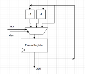
This week, I worked on the design report, writing the subsections under system implementation,  the test and validation section,  and the section on ethical and societal considerations. This helped me better think through the design for the various modules, and start drafting up block diagrams for them. Additionally, I wrote the RTL for the delay module in the system. I designed an additional param_register submodule to store the parameters, allowing for basic manipulation of the stored value, according to the following block diagram:

From here, the block diagram for the delay component was:

The multiplication operation was implemented using an on-chip DSP slice, since I assumed that any custom implementation would take far longer to create a circuit around the same speed. The DE10-Standard FPGA also contains double-ported BRAM, meaning that the concurrent read/write operation necessary for this component can be natively supported. Next week, I hope to implement the RTL for the IIR and FIR components.


Mihail’s Status Report for 2/21

This week I focused on implementing the RTL for the frequency modulation component of our digital synthesizer and began planning the ADSR envelope component.

For the FM component, I implemented a 24-bit phase accumulator to track the phase of the waveform. The circuit takes in a tuning word representing the carrier frequency, a modulation signal, and a scaling factor. It then uses them to update the phase accumulator every clock signal, outputting the modulated phase, which will then be used for wave table lookup. FM computation is coupled with the phase accumulator, so that we can ensure consistent behavior across output types.

Additionally, I began planning the ADSR envelope generator, mainly sketching out the finite state machine for the system. I also began writing Matlab scripts so that I could test simulation output of the FM component against a reference model, but had to spent most of my time brushing up on the language, since it has been about two years since I had used it.

Next week, I hope to verify the RTL for the frequency modulation component, sketch out the data path for the ADSR module,  and begin implementing the RTL for it.

Mihail’s Status Report for 02/14

This week I spent my time with the team, preparing the design presentation. I spent much of my time focused on the solution approach for the FPGA internals, particularly our audio processing pipeline. Additionally, I worked on creating a plan for testing and verification, looking at how we could numerically compare our digital output to a golden model, and responded to some feedback from the TA regarding the presentation. After next week’s presentations, I hope to get started on implementing the RTL for the frequency modulation and applying the ADSR envelope.