
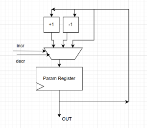
This week, I worked on the design report, writing the subsections under system implementation, the test and validation section, and the section on ethical and societal considerations. This helped me better think through the design for the various modules, and start drafting up block diagrams for them. Additionally, I wrote the RTL for the delay module in the system. I designed an additional param_register submodule to store the parameters, allowing for basic manipulation of the stored value, according to the following block diagram:
From here, the block diagram for the delay component was:
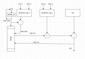
The multiplication operation was implemented using an on-chip DSP slice, since I assumed that any custom implementation would take far longer to create a circuit around the same speed. The DE10-Standard FPGA also contains double-ported BRAM, meaning that the concurrent read/write operation necessary for this component can be natively supported. Next week, I hope to implement the RTL for the IIR and FIR components.