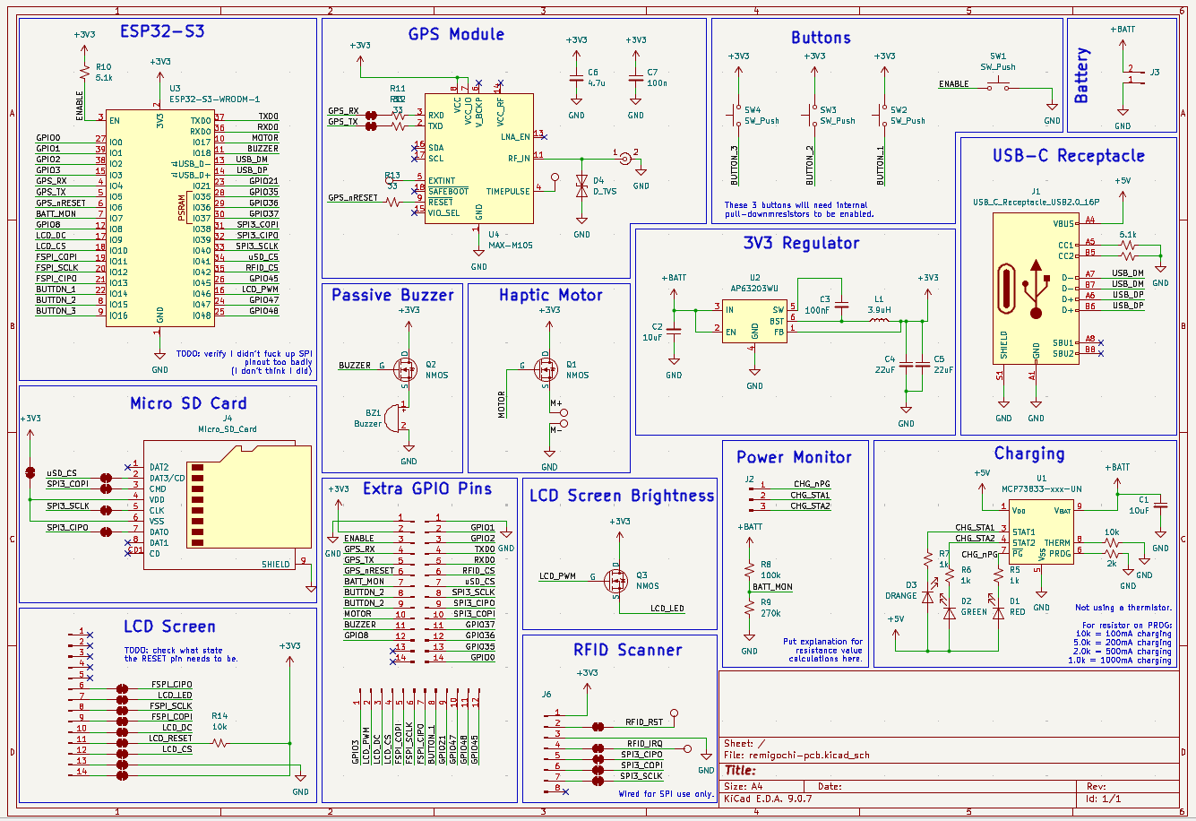
This week, I nearly completed the schematic. I just have a few questions regarding exactly how the pins on the LCD screen work, and once those are answered, I will be ready for layout.
While I am waiting for some answers (determined experimentally) on how the LCD screen pins work, I found and verified component footprints. This helps ensure that I don’t fall too far behind. Once I am confident of pin connections, I can begin layout right away. For this first spin of our PCB, layout and dimensions don’t need to be exact. This board is going to be a proof-of-concept, and we will order a second board once we are confident in the functionality of this electrical design.
To mitigate risk in this electrical design, I added additional breakout header pins to every connection on the microcontroller. Additionally, I put solder jumpers on all the connections to the auxiliary components. Therefore, it is easy to change a connection or pinout if we need to, and this design can have multiple functions.
Next week, I need to have the PCB ready to order before spring break!