
Accomplished:
This week, I focused heavily on device characterization and demo PCB integration. A large portion of my time was spent at the probe station performing transistor sweeps, CVU measurements related to switching behavior, and extensive resistance measurements across on-chip structures. This measurement work was important for giving Ethan the empirical data needed to support the V2 design iteration planned for tomorrow. In addition to collecting the data itself, I also spent significant time learning the probe station workflow in practice so that I could more efficiently support characterization needs as they came up.
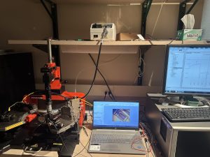
On the hardware side, I finalized the schematic for the demo PCB this week. With the schematic now complete, the remaining PCB work has shifted from circuit definition to physical layout and packaging in the design software. I was also effectively on call throughout the week to help both Ethan and Charlie whenever new data or measurement follow-up was needed, since characterization results were directly informing design and integration decisions.
Progress/Schedule:
I am currently on schedule for my portion of the project. This week was busy and fairly tight in terms of timing, but it was also productive in that the measurement work successfully produced data that can immediately feed into the next design iteration, and the demo PCB schematic has already been finalized. That means the project has continued moving forward on both the characterization and hardware integration fronts without falling behind schedule. At this point, the remaining PCB work is concentrated in layout, final packaging, and ordering on time.
Upcoming Deliverables:
For next week, my main priority is to complete the demo PCB layout and submit it for ordering by the Tuesday deadline. In parallel, I also need to finalize and order the remaining supporting materials for the demo setup, including items such as the voltage booster (MT3608), chip carrier, and any additional components still needed for assembly and testing. Beyond the PCB and parts ordering, I will continue supporting measurement and characterization work as needed so that I can quickly respond to results from Ethan’s end. My main deliverables for next week are to finish the PCB layout, ensure all remaining materials are ordered on time, and continue providing empirical support where needed for rapid iteration.