Andy’s Status Report for 03/13/2021

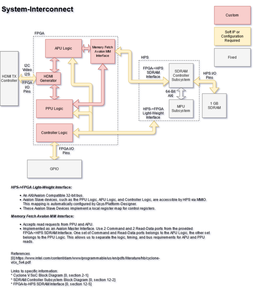
This week, my main task was to create the memory mapped I/O necessary to send controller input from the FPGA to the ARM core. In our design, we chose to use the lightweight AXI bus of the Cyclone V FPGA to accomplish this. Additionally, I set up my FPGA with a linux image that allows for a UART console and wrote a brief controller read program to test the communication. Finally, I set up an ARM cross-compilation development environment on my computer, using the arm-none-linux-gnueabihf library provided by arm, in order to compile the controller test program.


Under the current settings, the controller input is available to the ARM core at the base address of the lightweight AXI memory mapped I/O space (address 0xFF200000). The controller test uses /dev/mem to mmap this address into its address space and read from it, then prints the results to the console.


Due to my unfamiliarity with qsys, the process of bringing up this communication took longer than I expected. When all was said and done, I did manage to get communication working, though I ran out of time and was unable to finish the controller section of our interface (which would require wrapping it in a kernel module which has a call safely exposed to the user and definitions to ease in parsing buttons). Due to this, I’m slightly behind, but anticipate being able to catch up again next week.


A video of me running the controller test is available here: https://www.youtube.com/watch?v=jU2mdtBN-I0


The controller test:

https://drive.google.com/file/d/1U8mn_7gTbG2sWP3rkUN0vx-6YtHiBfZu/view?usp=sharing

Joseph’s Status Report for 3/6/21

I spent time early on in the week learning about the bus interfaces that the DE10-Nano development environment provides as soft IP. Intel has an hour and a half video on the subject that I took notes on:
https://www.youtube.com/watch?v=Vw2_1pqa2h0

These notes include the most important elements to discuss during next week’s team meetings:
http://course.ece.cmu.edu/~ece500/projects/s21-teamc1/wp-content/uploads/sites/133/2021/03/Tools-Platform-Designer-Updated-3-6-21.pdf

These bus interfaces will be extremely important for us next week when we begin to implement DRAM fetching and HPS to FPGA communication.

On Thursday and Friday, I did research on I2C configuration of HDMI. This is important as we want to change the video and audio data formats from their defaults. To study I2C configuration of HDMI, I modified the HDMI_TX demo and read the ADV7513 programming/hardware guides. I’ve included my notes on this below. Warning: the notes have unfinished sections with highlights to remind myself to look into them after this status report is due.
http://course.ece.cmu.edu/~ece500/projects/s21-teamc1/wp-content/uploads/sites/133/2021/03/I2C-Config-Updated-3-6-21.pdf

On Friday and Saturday, I began preparation of various system diagrams. I’ve included links to the diagrams and their notes below.

System-Interconnect Diagram:
http://course.ece.cmu.edu/~ece500/projects/s21-teamc1/wp-content/uploads/sites/133/2021/03/System-Interconnect.png

HDMI Config Diagram:
http://course.ece.cmu.edu/~ece500/projects/s21-teamc1/wp-content/uploads/sites/133/2021/03/HDMI_Config.png

HDMI Generator Diagram:
http://course.ece.cmu.edu/~ece500/projects/s21-teamc1/wp-content/uploads/sites/133/2021/03/HDMI-Generator.png

Team Status Report for 3/6/21

This week, we mainly focused on the interfaces between our modules and their internal structure in preparation for the design review. We defined what the MMIO interface will look like for our project, though the syscall interface is still a work in progress. We also generated block diagrams for all of the FPGA components of our system.

We’ve also made some major shifts in the general structure of our project. In particular, we will no longer be building a custom kernel for our FPGA. This decision was made for a few reasons. First, it negates a significant amount of risk involved in bringing up our system, as creating the kernel ourselves would have pushed back a large amount of testing. Second, it removes a large burden from us, and gives us time to create a full game to demo the functionality of our system. Finally, it allows us to easily provide the user with the full C standard. Note that this decision means our system call interface is actually now a kernel module interface.

Finally, in light of these changes and what actually was accomplished this week, our schedule has been drastically changed. The details of these changes are below. Under these new changes, we’re right on schedule and expect to be able to maintain this schedule without causing excess stress for either of us.

Schedule Changes:

  • Removed Kernel-related tasks from Schedule. We intend to use a customizable Linux kernel instead.
  • Added CPU task for development of the test game before interim demo.
  • Removed PPU tasks for foreground scrolling and layering for foreground and sprites. The foreground tile engine is a copy-paste of the background tile engine. Layering will be accomplished with the sprite engine implementation.
  • Added another task to the PPU called DRAM Tile Fetch. This task will consist of implementing the Avalon MM Master on the PPU side to fetch tile data from DRAM.
  • Moved back input-related tasks. Andrew made good progress this week and we should be able to complete it earlier now.
  • Pushed back audio tasks by two weeks to make room for input tasks.
  • Pushed back implementation deadline of the PPU driver to until after the main PPU tasks are finished. Realistically, the PPU driver will be worked on in parallel with all of the PPU tasks for testing purposes.

Our updated Gantt Chart schedule can be found below:
http://course.ece.cmu.edu/~ece500/projects/s21-teamc1/wp-content/uploads/sites/133/2021/03/Project-Schedule-Gantt-Chart-Updated-3-6-2021.pdf

Our MMIO notes from Wednesday have been uploaded below:
http://course.ece.cmu.edu/~ece500/projects/s21-teamc1/wp-content/uploads/sites/133/2021/03/Communications-Updated-3-6-21.pdf

Our PPU diagram from Saturday:
PPU Diagram

Andy’s Status Report for 03/06/2021

This week, I documented the internal structure of the audio and controller modules, and created block diagrams for those modules. I also detailed the controller FSM to aid in the implementation of the controller module.

On the subject of the controller module, I implemented and tested that this week. The protocol has been detailed in previous reports, but essentially the module is a timer running at 60Hz and a clock divider that generates the clock for the controller. Once the timer fires, the FSM waits to sync up with the controller clock and then begins the input request protocol. As discussed before, the controller is wired over GPIO. In the tester, the current input state of the controller is displayed on the LEDs of the DE10-Nano. Since the DE10-Nano only has 8 LEDs, and the controller state is 16-bit, a switch 0 is mapped to switching between the MSB and LSB of the controller state. After a few bugs and re-familiarizing myself with system verilog, it works like a dream. The LEDs lit up in response to my input apparently immediately. Unfortunately, a few of the wires for my controller port fell apart while I was moving the board, so I didn’t get the chance to capture video of the demo (at any rate, the LEDs are small and probably won’t show up well anyway).

I’ve attached the controller and audio diagrams, as well as the controller module implementation and test source code. Note that we’re managing our code on a private github, and the tossing of zips is just to ease distribution over our blog.

Diagrams:

Audio

Controller

Controller test source code:

https://drive.google.com/file/d/1dZzLapQ6Y364X1jte-TLIdnNxRoFoYm6/view?usp=sharing

Joseph’s Status Report for 2/27/21

This week I did research on HDMI for our project. I specifically wanted to know what protocols/interfaces the PPU needed to support on the video output. Knowing this will help narrow down possibilities for an actual PPU design. For example, we can determine things like signal timings, clock rate, and other constraints that will get us started on designing and testing the Tile Engine and other PPU features.

The DE10-Nano uses an HDMI Transmitter Controller IC called ADV7513. The link below is the datasheet containing the general features and some electrical characteristics for the chip:
https://www.analog.com/media/en/technical-documentation/data-sheets/ADV7513.pdf

I logged my research notes on HDMI in a document. The resources page contains links to the various websites, datasheets, and manuals I used. The version for 2-27-2021 is linked below:
research_PPU_HDMI_2-27-21

To summarize the document:

  • There is an HDMI demo for the DE10-Nano which showcases a simple pattern graphics test and simple audio output.
  • Interestingly, it shows that we must interface with the ADV7513 using a VGA-like signal protocol (Horizontal Sync, Vertical Sync, Data Enable, 24 bits of RGB).
  • Even more interestingly, it may serve as a complete, standalone module to use with our other PPU features. This means we have the option to avoid dedicating time to the HDMI implementation if we reuse the implementation from the demo.

After reviewing the demo code for HDMI on the DE10-Nano, I decided to swap the HDMI-bring-up task on the schedule to this week and design the PPU interface next week. I still intend to work on the PPU interface this week (on Sunday 28th – past the due date of this post), however, ensuring that HDMI could be taken care of was more important for me so that I could begin to gauge what kinds of PPU designs were possible. This schedule swap was mainly done as a mitigation strategy to prevent HDMI implementation (something I am unfamiliar with) from becoming a problem later on in the project.

The last interesting note about this week: I reached out to the TAs and course staff Thursday to get the DE10-Nano boards ordered. I hope to get access to these boards early so that we can test our code on actual hardware as soon as we are able to write it.

I was unable to design the PPU interface this week, so I am slightly behind schedule. I still have time to do it on Sunday (28th), but I expect it to be completed regardless by the next status report.

Next week I will be finishing the PPU interface as well as helping to design the system call interface. We also will have to be careful and plan around the time we must spend on the design review presentation.

Team Status Report for 2/27/21

This week, we worked on our project proposal presentation and began working on a design for the implementation of our project. We decided to use the DE10-Nano to implement our console for several reasons:

  • It offers HDMI output, simplifying the implementation of sound generation and ensuring that video will be compatible with more devices.
  • It uses a Cyclone V FPGA, which includes an ARM core, meaning we don’t need to dedicate as much time to the communication between modules.
  • It has a large amount of ram and an SD card port, which the ARM core can boot from, meeting our storage requirements for ram and program storage.
  • It has GPIO pins, which will allow us to communicate with older video game controllers easily.


Additionally, we performed individual research into the design and implementation of our project. Due to an error in our schedule and several facts coming to light during our research, we had to rearrange our schedule a little. Overall, the project is slightly behind schedule, but expected to be back on schedule by the end of next week. Andy was unable to finish a design for the audio interface, but expects to have it done soon. Joseph was unable to complete the design for the PPU interface, but also expects to finish it quickly.


Schedule Changes:

  • Moved design presentations back a week. That was an error in our initial scheduling.
  • Moved system call design back a week, to fix the same error.
  • Joseph: Swapped the PPU interface design and HDMI tasks. Designing the PPU interface will be for next week (Mar. 1st).
  • Andy: APU interface design moved back a week (he’s behind schedule).
  • Andy: Input implementation moved back a week, as design time revealed that no more time would be needed and this allowed slack to be added to sprite engine implementation.


Our updated Gantt Chart schedule can be found below:

http://course.ece.cmu.edu/~ece500/projects/s21-teamc1/wp-content/uploads/sites/133/2021/02/Project-Schedule-Gantt-Chart-Updated-2-27-2021.pdf

Andy’s Status Report for 02/27/21

This week, aside from helping with the presentation and discussing the overall plan with Joseph, I worked on research for the Audio, Input, Software, and Communication systems. I’ve attached a copy of my notes.

Suffice it to say, the current plan for audio is to have a single channel of 8-bit PCM audio and 32KHz, which will be representative of the GBA in sound power. Note that our users will be able to produce better sound, as they aren’t bound to a 16MB cartridge, though. Audio will be output by sending samples supplied by the CPU over I2S to the HDMI output. The interface itself hasn’t been designed yet, as I’m not sold on how it should be done specifically, so I’m a touch behind. I plan to get that done as soon as possible, and I’m confident I can be back on track by the end of next week.

For input, we plan to use a SNES controller over GPIO. I go over the details of the SNES controller communication protocol in my notes. It’s a simple protocol thats clocked well below what our FPGA will be clocked at. It should be relatively simple to bring up, as long as we can find controller ports.

For software, I took another look at the C standard and realized that our requirement of providing it to the user is completely infeasible if we are also creating our own kernel. The C standard has a lot to say about what an OS should provide, and we won’t be providing much of it. I’ve narrowed it down to a useful subset, which is listed in my notes.

For communication, I spent way too much time trying to understand how the FPGA and HPS communicate with each other. From what I can gather, the last GB of the HPS’ address space is mapped to the HPS-to-FPGA AXI bridge, and reading from/writing to it will send a signal to the FPGA that it can interpret and respond to. I think I’ll have to run some experiments when I get my board to convince myself of this. I’ll also need to spend some more time with the Cyclone V manual, it seems.

Finally, I also wrote a small C program to convert 16-bit 32KHz Mono Microsoft PCM Wave audio to pure 8-bit samples. It works with all the wave files I’ve exported from audacity into this format, though I didn’t rigorously test it. I did this so that once the audio system is brought up, we have working audio to make a direct comparison against. The program will also output 8-bit wave form audio in the wave format, so that it can be played on a computer and compared to our FPGA’s output. The source code for the program has been attached as well, though I’ve not tried building it on Windows/Mac.

Program source

Design Notes

Joseph’s Status Report for 2/20/21

This past week I was tasked with doing research on retro-console audio. We specifically wanted to know:

    1. How is audio typically generated on retro consoles?
    2. What should our audio requirements be?

Firstly, I had gathered some great resources on retro console architecture, featuring several of Nintendo’s consoles. The sound specifications (along with some graphics and CPU specs) can also be found from these links:
https://www.copetti.org/writings/consoles/nes/
https://www.copetti.org/writings/consoles/game-boy-advance/

I had also found a good resource for the Game Boy sound interface from the software perspective:
https://gbdev.gg8.se/wiki/articles/Gameboy_sound_hardware

In short, the audio can be synthesized digitally using counters and a digital mixer implemented using adders. An implementation similar to the Game Boy Advance (GBA) seems feasible. To summarize the specifications for the GBA’s audio, there are 6 channels for digital sound synthesis:

  • 2 square wave generators with programmable frequency.
  • A noise channel.
  • An arbitrary waveform generator (which outputs a pre-programmed sequence of 4-bit samples).
  • 2 8-bit PCM channels.

After bringing these findings to the team meetings mid-week, we decided on requiring a single 8-bit PCM channel. This is the most feasible option given the heavier requirements of the graphics PPU.

I spent Friday night and Saturday morning setting up and customizing the project website.

I am currently on schedule. However, I still have to plan on the individual deliverables to complete next week.

Team Status Report for 2/20/21

Hello and welcome to our first team post!

This past week, we worked on nailing down our design requirements and scaling back our design to something which can be met within our time limit. The main changes in this area are to the Pixel Processing Unit (PPU) and Audio Processing Unit (APU).

For the APU, we now intend to implement something very similar to that of the Game Boy Advance (GBA), which merely offers buffered 8-bit samples to two DACs. We currently intend to provide mono output for this sound. This is simpler than designing several wave generators and an interface to manage them, while also giving our users more freedom in the sounds they can create using our console.

For the PPU, we decided that instead of implementing a subset of what the GBA offers we will instead design something new from the ground up. This gives us the freedom to meet our requirements in a way which is efficient for our time, and ensures that we can adjust the design to meet the requirements of the rest of our system. For example, we may require increased sprite size capabilities, compared to the GBA, as our display is larger.

Our requirements document (updated 2/20/21) can be found here:
http://course.ece.cmu.edu/~ece500/projects/s21-teamc1/wp-content/uploads/sites/133/2021/02/FP-GAme-Requirements-2-20-21.pdf

Andy’s Status Report for 2021-02-20

This past week, outside of our group meetings, I looked into what would become our requirements for the processor in our handheld. Previously, all we really had nailed down was that we wanted something Arm clocked at at least 16MHz. We can now specify some more detail on that.


Based on our projects overall goals of providing a safe development environment, we decided to create a small software kernel for our console. This means our processor must provide the tools to implement such a kernel, namely memory protection. Arm processors do offer memory protection, but as an optional component, so we’ll need to ensure that if we use an Arm processor it offers memory protection. We must also ensure that any processor we use allows us to externally send interrupts to it. This will become important when managing our graphics and sound output. Finally, we’ll need a timing register to allow our kernel to support some basic timing facilities. Currently, I think our best bet is to simply expose a configurable timing interrupt to the user. Such an interrupt would hand off to some user provided function in a specified interval and allow the user to perform some time sensitive operations. Doing so would allow the user to track the passage of time and perform time based actions like multi-threaded code, should they wish to. Due to timing constraints, providing the user with a full threading library is outside the scope of our project.


Additionally, I also was able to get more firm requirements on the memory of our console. The GBA offers 256KB of slow ram + 32KB of fast ram, with the latter often used to cache full arm instructions as it was the only ram in the console to use a 32-bit bus. Since our project is aiming to provide a similar experience to consoles like the GBA, we must provide at least 512KB of ram. Since we’ll be including a kernel with our console, we should provide more than that, likely closer to a megabyte. In any case, I doubt this requirement will be difficult to meet. The more interesting one is the long term storage requirement. GBA cartridges ranged in size from 4MB to 32MB. We’ll need to ensure that our console offers long term storage in this range, and preferably said storage will not be unbearably slow. One option could be to ensure that we find an FPGA which offers at least this much flash storage.


At this moment, we’re right on schedule. In this next week, we will finish off our proposal presentation and research the hardware we will use for our project.


The basic GBA hardware information was obtained here:

https://www.copetti.org/writings/consoles/game-boy-advance/


The cartridge size information was obtained from here:

https://projectpokemon.org/home/forums/topic/22987-what-are-all-possible-rom-sizes-for-clean-dumps-gb-gbc-gba-nds/