Jared’s Status Report for Apr 25

Integration is finishing up both with the host and with the data pipeline router.
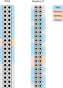
Host to Bus

With the host using UDP only for the finder, the Pi has both a UDP server for being found and a TCP server for receiving data. The TCP server follows RCE-style order, where every sent command is followed by a response.  The host prepends the length of the message, so that the Pi and bus can detect the length at the start of the command.
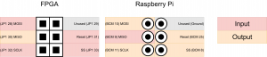
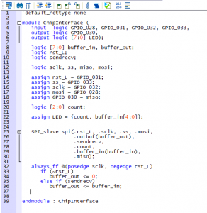
Bus to Hardware

TJ gave me the code to the memory model. The bus morphs this into streaming an incoming command, where instead of waiting for read enable, it raises “done” every time a command is received. As the hardware is in charge of copying commands to an assigned location, the hardware keeps up with the bus.

Integration needs to be solidified with the host and I am in contact with TJ to help him complete hardware integration.

Jared’s Status Report for Apr 18

The SPI bus is done. It operates at 15.6 MHz and transfers the data to and from the 50MHz domain successfully. The current protocol is as follows:

If the Pi receives a command:
Transfer a single byte (value 0x1).
Transfer the message length (size 4 bytes).
Transfer the message
Wait for single byte (value 0x1).
Read in the message length (size 4 bytes).
Read the message.
Transfer the message to the original sender.

The routine requires that every message has a response. A possible addition to this is a routine that attempts a short SPI read when receiving an empty message.

A recent change in design was made to use TCP over UDP. At the time I did not realize it, but the protocol does not interpret message fragmenting correctly. While we did not integrate in time to reach this state, I believe it would have caused issues on operation.

Jared’s Status Report for Apr 11

After meeting with a professor, I have determined that the SPI clock cannot run as fast as I expected. However, SPI is still the fastest method to transfer data.

What has changed is that the SPI clock will run at 15.6 MHz, or 250MHz / 16. This means that the 50MHz FPGA clock can successfully process the SPI clock without relying on a separate clock. I still have to code this, but it will be done by Monday.

By Friday, I plan to finish all of the SPI bus and spend the weekend completing additional tasks for TJ.

Jared’s Status Report for April 4

Placing the program on the FPGA isn’t as easy as I thought it would be.

Things that were easy:

  • Following the user manual and learning pin assignments
  • writing a compliant SPI module

Things that are hard:

  • Deciphering the signals from the RPi
  • Receiving the signals correctly

Here is my current configuration for the physical board:

Followed by a screenshot in Quartus of the interface (while debugging):

The SPI module likes to act strange: Once in a while it will count too many clock cycles and receive or return a bad buffer. This doesn’t appear when connecting MISO and MOSI together (loopback), so it must be with the Pi.

I have contacted sources outside the group for help, as without an oscilloscope I don’t think I can properly assess my issue.

Next week will be dedicated to getting SPI working.

Jared’s Status Report for Mar. 28

This week I wrote an initial draft of the SPI slave SystemVerilog code. Todo is the code to faciliate data transfer betwenn the Ethernet and SPI. This should meet the mark where we can put our pieces together, however I would still need to write some tests.

I received the parts for the setup this week. I will be connecting them to the host desktop for us to use and test on.

In relation to TJ I have been slacking a bit on code. I hope to meet with him once this section is done and work on the meat and bones of the project a bit more.

Jared’s Status Report for Mar. 21

With the recent events, retrieving the DE0-Nano for testing after spring break wasn’t possible. While we are able to put together some of the initial hardware, we have dedicated work to verification of the code. As such, the validation will be split into two sections:

1. RPi Ethernet packet transfer
This test is essentially the program itself. A dummy routine will replace the SPI protocol in order to verify that packets are correctly processed.

2. FPGA data transfer
The RPi is communicating through SPI bus, which is thankfully incredibly easy to mimic in verilog. A testbench will require validating both sending and receiving data across the clock domains (125 MHz from SPI, 50 MHz from the DE0-Nano).

The RPi does not need a SPI test, as an external library handles the read and write calls.

This is incredibly behind schedule, but we live in incredible times. I’ll make sure to at least get the RPi Ethernet packet transfer test working.

On a side note, I am repurposing an old desktop as a SSH server for the team. It and the Pi will have internet access. I am taking precautions for the Pi, as I am aware that having an open interface with the username “pi” is unwise.


Jared’s Status Report for Mar. 14

It’s the week of spring break, so this is a bit more concise.

We’re not going through with DE10-Nano SoC, so I’ll have to finish the SPI code soon.

A procedure for initializing the Pi 2B is finally realizable after finding one quirk: I’ve assumed this Pi had WiFi this whole time, explaining why I failed every time I’ve tried to debug it over WiFi. Because of this, progress was finally made in proper FPGA/SPI testing. Ethernet/SPI conversion is up next.

Our team has been a bit scrambled in terms of timeline, but now I realize I should finish this up as soon as possible. There are a few parts to the tasks ahead:

1. FPGA SPI protocol with cross clock-domain queueing
The only concern here are the size of the buffers required, but I’ll ask the team about that.

2. Ethernet-SPI packet conversion
This is purely converting the data to a packet and sending it to the host, and vice-versa. More buffering involved.

Once these are done I’ll have to help with more FPGA-focused tasks.


Jared’s Status Report for Feb. 29

Its time to get working on that ethernet, and with a couple shake-ups in the design there’s a new board on the radar: the DE10-Nano SoC. The DE10-Nano has an onboard ethernet PHY chip and is cheaper than the RPi/DE0-Nano setup, along with the Cyclone V chip being a generation ahead. This is possibly a major change in the bus protocol, so I’m reordering the tasks for the week ahead to focus on aspects relating to synthesization.

In terms of this week, I gave a presentation on machine learning. I don’t know anything about machine learning.

The RPi is giving me more trouble than its worth, and to connect to it I had to reformat it. So far this week I set up a simple test program for the GPIO and SPI bus via the bcm2835 library. No test on the FPGA yet, but I did get a loopback read/write to work.

This next week is dedicated to a few tasks: Deciding if the DE10-Nano SoC is fine to switch to (I’m favoring it) and writing some Verilog to test the SPI bus and obtain data. If we switch to the DE10, the code will form the implementation of the communication protocol.

Jared’s Status Report for Feb. 22

This week was about experimenting with the GPIO bus protocol, understanding shortcomings and learning about specialized hardware withing the Pi.

Accomplishments

I’ve started on some final documentation for the bus protocol. Initially there was pressure (at least from myself) to prioritize throughput. That hasn’t changed, but after some research on optimum speeds for GPIO, some decisions had to be made to make life simpler down the chain.

The custom bus protocol we earlier designed is likely being scrapped for the built-in SPI protocol. There are a few factors involved:
1. The custom protocol was clock agnostic, in which data was sent parallel with an activating bit. SPI, while not having built-in parallel data, may still have GPIO toggling transfer modes.
2. The optimum throughput rate was a best guess given throughput benchmarks from StackOverflow that may not properly reflect setting multiple GPIO. With the Pi’s SPI clock at a maximum rate of 125 MHz, a more reliable and debuggable interface will help in the future.

Schedule

This week, I need to write a program for the SPI interface and a test module to run on an FPGA. By Friday, the module needs to be done and tested.

Jared’s Status Report for Feb. 15

Status report is a bit late, isn’t it? Turns out reports aren’t due the day before returning to the lab.

Accomplishments

For the past week, I’ve been detailing the protocol for the physical connection between the FPGA and the accompanying Raspberry Pi. The protocol accounts for available GPIO on both devices and attempts to maximize throughput from the Pi to the FPGA.

The document detailing the physical setup is here:

https://drive.google.com/open?id=12h_0X_CB3D_IyGUgf5_b_YGxSVW09nrvIl3oF7lknj8

The core supplemental diagram illustrates the GPIO on each board:

This design uses every GPIO pin on the Raspberry Pi. For convenience, The data pins are joined by direction, split across the send/receive notification pins.

Schedule

This week has a lot riding behind it: according to our Gantt chart, this week we determine if our ethernet implementation is viable. To test this , I need to mess with the DE2-115 boards and get an echo server running over GPIO. This server is likely going to form the backbone of our communication with the FPGA, as we’re limiting the effectiveness of the RPi to act as an alternative Ethernet PHY board. If all goes well, I’ll have something to write about. If all doesn’t go well, I’ll have something to write about.