Wes’ Status Report for 10/03/2026

3rd October 2026

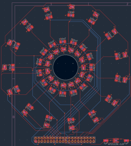
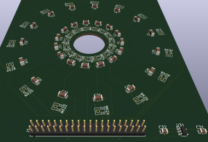
Added M2 mounting holes to the PCB (2.2mm diameter). Verified that all placement and routing on PCB design is correct and complete. Submitted the JLCPCB order for the minimum 5pcs, as well as all surface-mount / through hole components for the PCB:

1.       1 µF ±20% 50V Ceramic Capacitor X5R 0805 (2012 Metric)

2.       Linear Voltage Regulator IC Positive Fixed 1 Output 600mA SOT-25 (AP2112K-1.8TRG1)

3.       0.1 µF ±5% 50V Ceramic Capacitor C0G, NP0 1206 (3216 Metric)

4.      Harwin M22-2022005 (through-hole pins)

5.      SamTec TCSD-20-D-06.00-01-N (ribbon cable for connecting PCB to FPGA)

6.      SPH0641LU4H-1 Knowles Microphone

Worked on the design report, specifically on the justification for the microphone array design. Added all required equations for deriving the expected sound pressure level at a range of 10 feet, as well as array aperture sizing for angular resolution. Also added all equations justifying the design choice of the SPH0641LU4H-1 Knowles Microphone, deriving the self-noise floor of the microphone, and the operational signal-to-noise ratio picked up by the microphone array (after beamforming).

Goals for next week:

Wait for the arrival of the fabricated PCB and all the components, for surface-mount and through-hole soldering. This will be done in the TechSpark PCB Lab. After PCB assembly, to individually test every microphone for a data signal, before handing it off to teammates for the RTL bringup.
Wes’ Status Report for 09/26/2026

26 September 2026

Designed power subsystem for the device, which included estimation of the power consumption of each electrical component. From the system power consumption, I derived a required battery capacity to sustain 2 hours of operation. From that, I chose a 20000mAh power bank to provide 65W of power, enough to avoid any brownouts at 12V, 4A of current draw. Also designed the interface for getting power to the Ultra96-V2, which went through a USB-C to 5.5mm x 2.1mm barrel jack adapter, as well as another adapter to the required 4.75mm x 1.7mm port on the Ultra96-V2.

Quantified all design requirements for the microphone array subsystem, which included equations to derive the sound pressure level created by a gas leak, and the microphone signal to noise ratio (SNR) required for range detection. Also derived the array aperture required for angular resolution of two different leaks. All these quantitative derviations are in the Design Report.

Finalized the PCB components required (the microphones themselves, the exact models of capacitors to use). Downloaded KiCad and designed the schematic for the components. Place and routed the components on the PCB layout, ran Design Rule Check (DRC) to verify that all components are connected. Created gerber files and got a price quotation from JLCPCB ($30) for 5 pieces of PCB.

Schedule Status

The physical hardware implementation is on track, with the PCB design complete. Since PCB fabrication and shipping will take some time, this will be done in parallel with the shipping of other physical components (camera, LCD screen etc.) On track to receiving all materials and starting the build process right after fall break.

Goals for next week:

Verify that PCB schematic and layout is correct (visual inspection of all traces and connections) before sending it out for fabrication. Work on refining the design report. Begin purchasing the components required for the assembly of a prototype.

Wes’ Status Report for 09/20/2026

20 September 2026

I primarily worked on researching the geometries required for the 32-microphone array. I then produced the .scr file for Fusion360 Electronics (the PCB design), which took into account PCB routing constraints (such as the placement of the solder pads). I consolidated the “Materials” excel sheet for peripherals that interface with the Ultra96-V2 (camera, LCD display etc.), which included information such as:

  1. Cost
  2. Quantity
  3. Purchase Link
  4. Justification for order

Goals for next week

Place required components onto the schematic in Fusion360, then run all wire routing across all layers of the PCB (including 5V, ground planes). Run DRC and LVS checks across entire PCB board.

Then, submit the order to JLCPCB for a price quotation. Afterwards, submit the 18500 Purchase Request form (sharing the password to the account).