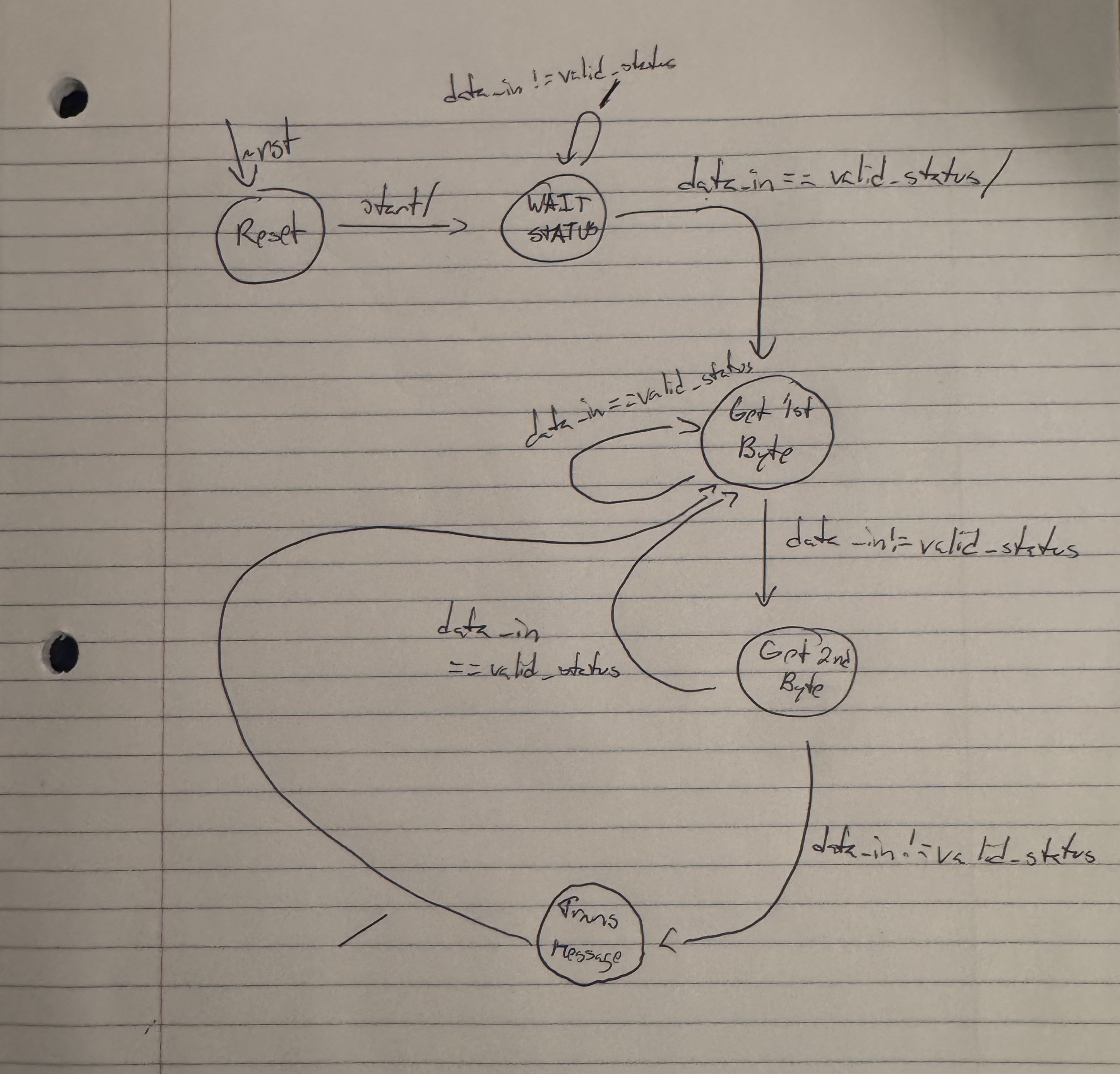
I spent this week working on the design/code for the FPGA’s audio codec. The following is split into two portions. The first has to do with the I2C protocol/wires that communicate with the CODEC. It’s impossible to ignore since it’s what needs to be utilized to send out the reset/power/setup write commands. With that in mind, I designed two handshaking FSMs for the purposes of 1. Sending out write commands for initializing the CODEC and 2. Handling the I2C protocol itself (i.e., sending out all the bits of data properly). The design for such FSMs can be seen below:
- I2C Protocol

This takes care to respect the I2C rules, particularly modifying the clock (which we provide) carefully when initiating data transfer. Just to note, the design also takes care of the fact that we’re transferring data at 100Khz (while the FPGA’s provided clock is going at 50Mhz).
2. Sending out commands

While the register we’re writing to is the same for all of these (address 0x34), the commands being sent all have unique hex values.
This was coupled with the actual interface with the CODEC, which was much simpler to implement since, apart from feeding the necessary clocks, data transfer is done through a parallel shift register.
This leads to an overall interface that looks like so:

Once all of that was done, I focused on setting up Quartus on my laptop for actually putting the code onto the FPGA and begin testing. While arduous, I got the pins set up and the entire system set to begin doing the previously described work next week.
My progress is on schedule, as I’d marked this week for developing the initial design/code for the system and next week for debugging/testing the code as necessary. With that in mind, I hope to get a system in which some sort of audible noise is heard next week implemented on the FPGA itself (now that my Quartus is set up properly).