Team report:
Changes to schedule:
We’re slightly behind on the hardware side of things because we only acquired our board this late this week, but our design has been simplified due to the use of an ARM core over a Microblaze and the Wi-Fi module being supported by the board rather than by us. This should cut some time out of interface bring-up and allow Ilan to help Edric a bit more with the pipeline design and implementation details.
As for the software side, Brandon’s slowly catching up after being very behind last week. He’s added the benchmarking to the Gantt chart for this week along with starting video frame/feed functionality.
Major project changes:
Possibility of full edge detection not being implemented in hardware due to limited number of DSP slices on the board. This would most likely mean we’d implement the first few stages in hardware, which are also the more computationally intense ones, and then move the data back to software. Once we implement the first stage and actually see how many DSP slices are actually used (as opposed to our theoretical calculations), we’ll know whether this change will happen or not.
Brandon:
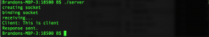
For the second week of work on the project, we were able to clarify our project significantly from the prior week. We’ve settled on a security system implementation with canny edge detection, and this means that most of our communication protocol design will stay the same. Thus, I was able to spend my time this week actually working on relevant code for the UDP protocol. I drafted up a test server/client to ensure that I could get basic UDP functionality working, which I was able to as shown in the pictures below. Some technical challenges I was able to overcome include some bugs with the server code that involved some MSG flags that I wasn’t setting properly, along with some sizing issues with the char array that I was trying to send. The steps I took to accomplish this was a lot of online research and talking with some peers. Once I got this working, I was supposed to work on reconfiguring my code to accommodate video streams, but instead, since we have our design presentation this next week, I’m currently trying to benchmark some latency numbers for sending a 1280×720 video frame, so I’m designing a chunking/packing algo and trying to time it.
With this new task, I am now slightly behind schedule, but not as much as I was last week. I’ve caught up on the UDP functionality, but haven’t started video streaming functionality yet, which I was supposed to do this week. In order to catch up, I’m going to try to finish both benchmarking and start video streaming functionality this week. These are the deliverables I hope to complete in the next week.
![]()
Ilan
Personal accomplishments this week:
- Decided on and acquired FPGA hardware. We’ll be using the Ultra96 with an ARM core and FPGA.
- No significant challenges here
- Steps involved mainly narrowing down between Zynq and Ultra96 due to ARM core, but Zynq was unavailable
- Future work involves board bring-up and interface development
- Researched steps of Canny edge detection in-depth with Edric, determined that it may not be computationally feasible to fully compute 2 simultaneous 720p streams on the FPGA due to limited number of DSP slices (360 slices total, so if 2 separate compute blocks would be used that would mean 180 slices/stream), or it may be quite tight to the 100 ms latency. Back of the envelope math shows it would take ~27 ms to do 3 convolutions (just in the first 2 out of 5 stages of the edge detection algorithm alone) in a pixel-by-pixel fashion, with each convolution using 9 DSP slices. If we want a pipelined design, each DSP slice will be dedicated to a stage, and so that alone allocates 27/180 slices for a single stream. This is something we’ll nail down once we implement the Gaussian filter, since that will require a convolution and will heavily inform how we implement the intensity gradient calculation (another 2 convolutions). At that point, we’ll have a definite answer as to under what timing condition we can fit the whole algorithm in the FPGA fabric.
- Technical challenges met were lack of familiarity with the algorithm, and some gaps in understanding specific stages
- Steps involved starting mainly by focusing on first 2 stages since these seem to be a significant portion of the algorithm in terms of computational time. Broke down computation performed by convolution based on DSP slices on FPGA and determined conservatively how we would use the DSP slice to determine frequency, computation time, etc.
- Future work will be when Edric implements first stage and sees how convolution ultimately consumes DSP slices
- Finalized interfacing design between ARM core and FPGA with Edric. We discussed all of the interfaces we’ll need and how those will work to allow the computation to be offloaded from the ARM core to the FPGA and read back once the computation has finished. We’ll section off a portion of DRAM for each stream, and use GPIO pins between the ARM core and PL to communicate status and control signals for the edge detection start/end. Since computing a matrix convolution efficiently means not overwriting the current data, we came up with 2 strategies for moving data between stages of the edge detection pipeline, 1 of which is our main strategy. Our main strategy is to allocate separate chunks in DRAM for each stage, so we can pipeline the design. This incurs more memory overhead, but based on our calculations it is feasible.
- No significant technical challenges here
- Steps were determine what interfaces we could use and what suited the application the best
- Future work will be myself implementing these interfaces
Progress on schedule:
- Edric and I made good progress on the edge detection pipeline design and interfacing, which is approximately on schedule.
- We didn’t have the power cable for the Ultra96 and couldn’t find a matching one in Hamerschlag, so I couldn’t do any quick testing of the board, which is slightly behind where I wanted to be. However, our previous schedule and architecture was based on using a Microblaze core, and after adjusting our schedule based on our finalized board decision the schedule hasn’t been affected.
Deliverables next week:
- Enabling basic ARM core and FPGA functionality
- Unblocks Brandon’s development and testing on the server-side
- Unblocks Edric to start flashing bitstreams onto the FPGA (not necessary for a while though, most designs will be simulated and only synthesized for timing and resource usage.
- No expected risk/challenge here, these tasks are mainly focusing on getting very basic functionality working and making sure everything is usable and set up for the future when things become more fast-paced
Edric
This week, because we managed to decide on and get ahold of our FPGA we could begin some estimates. On the hardware end, no code has been written yet, but we’ve managed to flesh out a few aspects of our design:
- Data coming from video streams will be placed in DRAM by the ARM core at a specified address
- DRAM address space is split into segments, where each stream is allocated a chunk of the space
- Once in memory, the ARM core will communicate to the fabric (compute blocks) that there is a frame ready for processing
- Simple consumer-producer protocol: core will ping fabric that a frame is ready, as well as what address the start of the frame is located
- When the frame is processed (and put back into DRAM), then the fabric will ping the ARM core that it is ready
Regarding the implementation of the Canny algorithm, there we’ve come across a few issues with respect to the actual implementation. It seems like we’ll need to do more work in trying to understand what operations are necessary, although focusing on the Gaussian filter for the time being seems reasonable.
We have, however designed the basic flow of a frame being processed (and how each step translates to its Canny algorithm step). This can be illustrated with the following diagram:
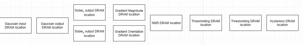
Each block represents a chunk of memory a copy of the frame (at each step) is located in DRAM. Unfortunately we can’t really edit the frame in-place, so this is how we’ll do it (for now).
Some foreseen challenges:
- Still need to figure out how the Canny algorithm works
- When there is both a frame done and a frame pending for processing, we’ll need to figure out a way to prevent deadlock between the producer (FPGA fabric) and consumer (ARM core)
- Perhaps a FIFO is enough. Will need to give it more thought.
For the most part, we’re a bit behind schedule, but definitely in a better place than last week. The next steps are to get flashing lights on the Ultra96, look into the Canny algorithm more, and perhaps solidify more our testing suite for looking at the output from the FPGA.