Sabah’s Status Report for 10/10

This past week, I finished the schematic and layout for the 8×8 PCB matrix. The layout took a lot of time because this was my first project in Fusion in about two years, so I spent time relearning the tools and wiring rules.

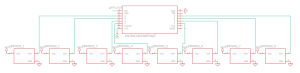
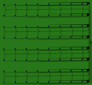
Here are the final schematic and the 3D layout:

8x8Digital SensorSchem

Our progress is slightly behind schedule. I decided not to send out the PCB before fall break, which technically set us back a full week. The PCB total came to about $364.50 (not including shipping), and we also need $25 for a stencil. That leaves roughly $30 in the budget for the NeoPixels, board materials, and chess pieces. While reviewing the order, we noticed a large $228.60 charge that came purely from the board’s size. We therefore decided to reduce the board from 2.5 x 2.5 inches per square to 1.1 x 1.1 inches per square. This lowers our cost and also helps our users, as a smaller board means less space for a visually impaired player to cover with their hands.

Over break, I have been shrinking the board and redoing the entire layout. To catch up, I rearranged some tasks. Instead of integrating the PCB next week, I will work on the front end of the website and on ordering and wiring the NeoPixels. By Monday, I hope to have the orders for the PCB and NeoPixels confirmed. For the rest of the week, I will figure out how the NeoPixels will work with the Jetson and begin work on the website.

Sabah’s Status Report for 10/3

This week, I spent a lot of time practicing for the design presentation. In addition, I completed the matrix schematics for both the analog and digital sensor matrices. Here are the specs/connections of the sensor matrix: 

Analog Sensor Matrix: 
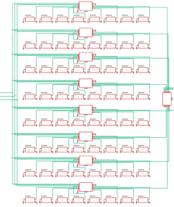
There are 8 sensors per row. Each sensor connects to a “mini” mux, and the 8 mini muxes feed into the master mux. The mini muxes share the same S0-S2 lines, while the master mux gets its own control lines.

For each mini mux:

A0-A1 Sensor0-Sensor7
S0-S3 Jetson GPIO inputs (control lines) (shared)
A Master Mux (first row mini mux A corresponds to A0 of master mux)

For Master Mux: 

A0-A1 MiniMuxRow0 – MiniMuxRow7
S’0-S’3 Jetson GPIO inputs (control lines) 
A ADC Input 
ADC Output  Jetson I2C Ports 

The Nvidia Jetson will have 6 GPIO ports for the designated control lines. The first three (S0, S1, S2) are connected to the S0, S1, and S2 ports of all the mini muxes. The next three (S’0, S’1, S’2) are connected to the S0, S1, and S2 ports of the master mux. The S0-S2 lines choose the column from each row, and then these 8 column sensor values, one from each row, go into the master mux. The master mux will then choose each row one by one and send each value into the ADC, then into the I2C ports of the Nvidia Jetson.

Here is some pseudo code for how the matrix will work: 

For c in range(0,7): # choose column for each row [c0, c1, c2, c3, c4, c5, c6, c7]^T

     For r in range(0,7): # choses the row from the set of columns   

          Return matrix[i,j]

Digital Sensor Matrix: 
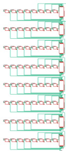
In this matrix, there are 8 shift registers, one for each row. The shift register is a PISO, so it will take in all 8 sensor results in parallel and pass them out serially through one data output line (QH). This matrix works by daisy-chaining the shift registers together in order (SR0’s QH goes into SR1’s SER). The final output will be a serial line (from SR7’s QH) of 64 digital values, either 1 or 0. The first digit of the 64 will be for Sensor 0 in Row 0, and the last digit will be for Sensor 7 in Row 7.

In terms of the schedule, which has been changed for the design presentation, I am on track with completing my task for building the Hall sensor schematics (8×8), as shown above. However, our team task of testing the sensors and physical board has been pushed to next week because we just received the sensors on Wednesday and are not able to test them until Monday. I think as long as we complete the testing on Monday, I will be able to complete next week’s task of laying out the Hall sensor matrix after we have chosen which sensor to move forward with.

For next week, I plan to lay out the chosen sensor matrix and implement the LED matrix. Then, over the weekend, I should be able to order the full PCB.

Monday:

  • Run sensor tests
  • Discuss board dimensions

Tuesday-Thursday:

  • Layout board based on dimensions (LED & SENSOR)
  • Do final connection checks (power lines/register or mux connections/capacitors where needed)
  • Add to cart and calculate cost

Wednesday/Thursday:

  • Discuss with TA and send out the order if possible

I want to try my best to get the order out by Wednesday since the following week will be fall break and we don’t want to delay our pcb order. 
Sabah’s Status Report for 9/26

After a conversation with my TA, I realized the best course of action was to actually test out both sensor types rather than decide based purely on specs, especially considering potential magnetic cross-talk across adjacent squares. So, I have ordered a test-bunch (8 each) of both the digital and analog sensor alongside the exact magnets we will be using for the final project. Hence, testing will begin as soon as these materials arrive. In the meantime, we received our NVIDIA Jetson Orin Nano. This lets me establish exact hardware pin mappings which is helpful for considering how many GPIO ports I will have from the PCB. 

Since we are not sure about the sensors yet to stay on schedule, I developed the plan for two distinct 1×8 array PCB layouts. For our digital approach, I am pairing eight DRV5032FADBZR Hall-effect sensors with a 74HC165 Parallel-In/Serial-Out (PISO) shift register. I specifically chose a PISO register over a Parallel-In/Parallel-Out (PIPO), because a PIPO register has 8 output lines, while the PISO register has an output of a single serial data line. When scaled to an 8×8 matrix, daisy-chaining eight shift registers end-to-end allows us to read all 64 squares across the board while only using 3 control lines (data-out, clock, latch). 

For the analog validation design, I am pairing eight DRV5055A1QDBZR linear sensors with a CD74HC4051 analog multiplexer. Using three digital GPIO selection lines we can choose from (000 to 111) for the multiplexer choosing between sensor 0 and sensor 7. Although Jetson Orin Nano doesn’t have built-in analog-to-digital converter pins, so the multiplexer has to be routed to an ADC chip (converts analog to digital number) before transmitting the data to the Jetson over I2C or SPI pins. To scale this approach to an 8×8 board, I plan to implement a two-stage multiplexing. Each row of 8 sensors gets its own CD74HC4051 analog multiplexer. The three digital GPIO selection lines will be in relation to the columns, so if 111 is chosen then the column 8 sensor for each row will be selected. Then these 8 outputs go into a master multiplexer which is chosen through another three GPIO selection lines. This essentially results in a nested for loop one for the column, and the other for the row. 

I am on time with the schedule, as we have ordered all necessary components and I have designed the plan/schematic for the 1×8 architecture. I should be done with the PCB 1×8 prototype by next week. In addition I will be presenting for the design presentation next week, so I will be spending some time preparing for that. I hope to deliver that well :). 

Digital:

Analog:

When implementing the ADC (ADS1115IDGSR) , port (A) from the multiplexer will be allocated to the ADC.

Sabah’s Status Report for 9/19

This past week, I spent time finalizing the system’s circuit architecture, researching components, and planning my approach for the PCB. The final PCB board will use an 8 × 8 matrix of Hall-effect sensors and LEDs, but I decided to begin with a 1 × 8 prototype. This will allow me to confirm that the sensors work properly and meet our 98% accuracy user requirement before ordering the complete board. A major concern is crosstalk, where a magnet may activate a sensor on a neighboring square. I compared linear analog sensors, which measure magnetic-field strength, with switch sensors, which produce a simple ON/OFF output. Although analog sensors could help identify which sensor has the strongest reading, they would require more processing and could increase latency (another user requirement). Since both accuracy and response time are important, I decided to use a switch sensor. I selected the 20 Hz DRV5032 digital omnipolar switch because it is sensitive, responds quickly, and is omnipolar. I also want to test the sensors physically before finalizing the PCB, so I plan to purchase/find SOT-23-to-3-pin DIP breakout boards. These will allow me to connect the sensors to a breadboard and test the complete 1 × 8 setup using an Arduino. 

I am slightly behind schedule, although I completed this week’s main tasks: finalizing the circuit architecture and selecting the major components. The delay is mainly because I have not yet submitted the component order form. To catch up, I plan to meet with my TA on Monday to review my approach and component choices before submitting the form. Once the approach is approved, I will submit the order immediately and begin the PCB design while waiting for the components to arrive.

Next week, my main goal is to complete the 1 × 8 PCB array design by Friday. This includes designing both sides of the board, with the LEDs on the top and the Hall-effect sensors on the bottom. Since I have previous PCB design experience, I believe this is a realistic goal. In parallel, I also want to begin working on the design presentation, which is due next weekend. I will be presenting on behalf of my team, so I want to discuss each part of it with my teammates.