This week, I spent a lot of time practicing for the design presentation. In addition, I completed the matrix schematics for both the analog and digital sensor matrices. Here are the specs/connections of the sensor matrix:
Analog Sensor Matrix:
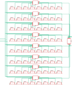
There are 8 sensors per row. Each sensor connects to a “mini” mux, and the 8 mini muxes feed into the master mux. The mini muxes share the same S0-S2 lines, while the master mux gets its own control lines.
For each mini mux:
| A0-A1 | Sensor0-Sensor7 |
| S0-S3 | Jetson GPIO inputs (control lines) (shared) |
| A | Master Mux (first row mini mux A corresponds to A0 of master mux) |
For Master Mux:
| A0-A1 | MiniMuxRow0 – MiniMuxRow7 |
| S’0-S’3 | Jetson GPIO inputs (control lines) |
| A | ADC Input |
| ADC Output | Jetson I2C Ports |
The Nvidia Jetson will have 6 GPIO ports for the designated control lines. The first three (S0, S1, S2) are connected to the S0, S1, and S2 ports of all the mini muxes. The next three (S’0, S’1, S’2) are connected to the S0, S1, and S2 ports of the master mux. The S0-S2 lines choose the column from each row, and then these 8 column sensor values, one from each row, go into the master mux. The master mux will then choose each row one by one and send each value into the ADC, then into the I2C ports of the Nvidia Jetson.
Here is some pseudo code for how the matrix will work:
For c in range(0,7): # choose column for each row [c0, c1, c2, c3, c4, c5, c6, c7]^T
For r in range(0,7): # choses the row from the set of columns
Return matrix[i,j]
Digital Sensor Matrix:
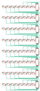
In this matrix, there are 8 shift registers, one for each row. The shift register is a PISO, so it will take in all 8 sensor results in parallel and pass them out serially through one data output line (QH). This matrix works by daisy-chaining the shift registers together in order (SR0’s QH goes into SR1’s SER). The final output will be a serial line (from SR7’s QH) of 64 digital values, either 1 or 0. The first digit of the 64 will be for Sensor 0 in Row 0, and the last digit will be for Sensor 7 in Row 7.
In terms of the schedule, which has been changed for the design presentation, I am on track with completing my task for building the Hall sensor schematics (8×8), as shown above. However, our team task of testing the sensors and physical board has been pushed to next week because we just received the sensors on Wednesday and are not able to test them until Monday. I think as long as we complete the testing on Monday, I will be able to complete next week’s task of laying out the Hall sensor matrix after we have chosen which sensor to move forward with.
For next week, I plan to lay out the chosen sensor matrix and implement the LED matrix. Then, over the weekend, I should be able to order the full PCB.
Monday:
- Run sensor tests
- Discuss board dimensions
Tuesday-Thursday:
- Layout board based on dimensions (LED & SENSOR)
- Do final connection checks (power lines/register or mux connections/capacitors where needed)
- Add to cart and calculate cost
Wednesday/Thursday:
- Discuss with TA and send out the order if possible
I want to try my best to get the order out by Wednesday since the following week will be fall break and we don’t want to delay our pcb order.