After a conversation with my TA, I realized the best course of action was to actually test out both sensor types rather than decide based purely on specs, especially considering potential magnetic cross-talk across adjacent squares. So, I have ordered a test-bunch (8 each) of both the digital and analog sensor alongside the exact magnets we will be using for the final project. Hence, testing will begin as soon as these materials arrive. In the meantime, we received our NVIDIA Jetson Orin Nano. This lets me establish exact hardware pin mappings which is helpful for considering how many GPIO ports I will have from the PCB.
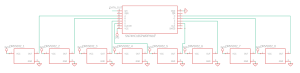
Since we are not sure about the sensors yet to stay on schedule, I developed the plan for two distinct 1×8 array PCB layouts. For our digital approach, I am pairing eight DRV5032FADBZR Hall-effect sensors with a 74HC165 Parallel-In/Serial-Out (PISO) shift register. I specifically chose a PISO register over a Parallel-In/Parallel-Out (PIPO), because a PIPO register has 8 output lines, while the PISO register has an output of a single serial data line. When scaled to an 8×8 matrix, daisy-chaining eight shift registers end-to-end allows us to read all 64 squares across the board while only using 3 control lines (data-out, clock, latch).
For the analog validation design, I am pairing eight DRV5055A1QDBZR linear sensors with a CD74HC4051 analog multiplexer. Using three digital GPIO selection lines we can choose from (000 to 111) for the multiplexer choosing between sensor 0 and sensor 7. Although Jetson Orin Nano doesn’t have built-in analog-to-digital converter pins, so the multiplexer has to be routed to an ADC chip (converts analog to digital number) before transmitting the data to the Jetson over I2C or SPI pins. To scale this approach to an 8×8 board, I plan to implement a two-stage multiplexing. Each row of 8 sensors gets its own CD74HC4051 analog multiplexer. The three digital GPIO selection lines will be in relation to the columns, so if 111 is chosen then the column 8 sensor for each row will be selected. Then these 8 outputs go into a master multiplexer which is chosen through another three GPIO selection lines. This essentially results in a nested for loop one for the column, and the other for the row.
I am on time with the schedule, as we have ordered all necessary components and I have designed the plan/schematic for the 1×8 architecture. I should be done with the PCB 1×8 prototype by next week. In addition I will be presenting for the design presentation next week, so I will be spending some time preparing for that. I hope to deliver that well :).
Digital:
Analog:

When implementing the ADC (ADS1115IDGSR) , port (A) from the multiplexer will be allocated to the ADC.