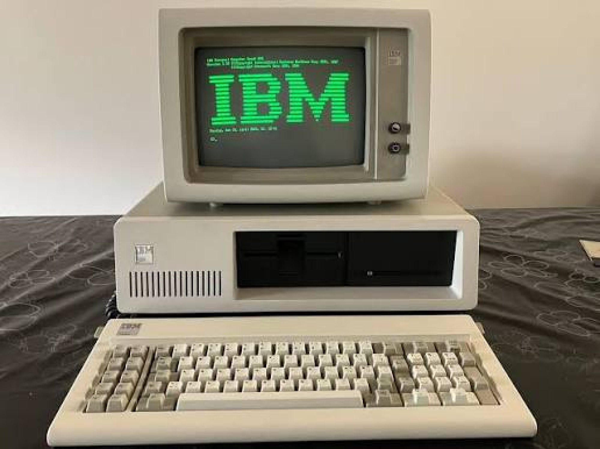
This week, I began RTL implementation of our custom CPU in SystemVerilog, building and verifying the first vertical slice of the datapath. I implemented and tested the general-purpose register file, including byte-register access. I also built an ALU that performs 16-bit ADD and generates all six status flags (carry, parity, auxiliary carry, zero, sign and overflow). It passed over 20,000 directed and reference-model checks. Next, I implemented a decoder subset for MOV r16, imm16 and register-to-register ADD. It consumes instruction bytes through a valid/accept handshake and waits correctly when bytes are unavailable or when execution is not ready. I then built an execution unit that connects the decoder, register file, ALU and writeback through a small instruction controller. The controller retains each instruction’s operation and destination until it finishes. The unit correctly executes a short demonstration program (MOV AX,3; MOV BX,4; ADD AX,BX; ADD AX,AX, leaving AX = 14) and a longer flag-focused program, and it stops safely on unsupported instructions. To check that the tests are meaningful, I injected deliberate bugs into each module and confirmed the testbenches catch them. This also exposed a remaining gap in the execution-unit tests that I will fix. I set up a repeatable local simulation flow with Vivado’s XSim and Make targets for each module, and recorded the test results. I also drafted the CPU-side bus ports (single-byte transactions with explicit completion, plus the interrupt inputs) for review with Ben. The CPU cannot yet fetch instructions from memory, so only these two instruction forms run, fed directly by a testbench. Next week, I plan to review the bus interface draft with Ben. I then plan to build the instruction fetch path (instruction pointer, segment registers, prefetch queue and a minimal bus interface unit) with a simulated memory model, so the CPU can run programs from memory. I will also start extending the decoder and ALU to the full family of arithmetic and logic instructions.
Ben’s Status Report (9/26)
This week, I split my time between working on our design presentation slides and continuing to refine the memory subsystem for our project. For the presentation, I helped improve the system architecture, requirements, testing plan, and overall organization of the slides so that the design and interfaces between the CPU, memory, peripherals, and software were clearly explained. On my individual work, I continued working through the CPU-to-memory interface, the initial RAM and BIOS ROM organization, and how address decoding will select between memory and peripheral accesses. I also started outlining the tests I will use for RAM reads and writes, ROM initialization, and address-decode boundaries before integrating with the CPU. My progress is currently on schedule, and next week I plan to finalize the CPU/memory interface with Josh, lock down the first version of the memory map, and begin implementing and testing the RAM, ROM, and address-decode modules before moving further into the storage and peripheral interfaces.
Team Status Report (09/19)
This week, the team focused primarily on completing the proposal presentation and turning the high-level project idea into more concrete CPU, memory/peripheral, and software designs. The biggest risks we currently see are integration between the three subsystems, correctness of the custom 8088 implementation, and making sure the software only depends on hardware and BIOS/DOS services that we actually support. To reduce integration risk, Josh and Ben are defining the CPU-to-memory interface early so that the processor and memory subsystem agree on request, response, and address behavior before RTL implementation progresses too far. Josh is also breaking the 8088 into smaller components and studying instruction execution, bus behavior, and interrupts so that individual pieces can be tested before full CPU integration. On the software side, Govind is identifying the BIOS and DOS calls needed by our target programs and plans to develop and test the software incrementally using MartyPC before moving onto the FPGA. If compatibility issues arise, our contingency is to narrow the required software set to programs that only use the interfaces we have implemented rather than expanding the hardware/software scope late in the semester.
We did not make a major change to the overall architecture this week, but we did clarify and refine several parts of the design while preparing the proposal. In particular, we more clearly defined .COM applications as our required executable target, while .EXE support remains a stretch goal. We also refined the boundaries between the CPU, memory/peripherals, and software and began defining the interfaces that will connect them. Ben started outlining the memory map, RAM/ROM structure, address decoding, and peripheral connections, Josh refined the CPU block diagram and bus interface, and Govind expanded the software design into BIOS device support, DOS services, program loading, and the shell. These refinements do not significantly increase the project cost, but they do require time up front to agree on interfaces and supported behavior. We expect that this will reduce integration and debugging time later in the semester.
The overall project schedule has not changed significantly. Next week, Josh and Ben plan to finalize the CPU/memory interface, define the first memory map, and begin implementing and testing the CPU, RAM, and ROM components. Govind plans to continue setting up the software development environment, verify the MartyPC workflow, and begin working toward the BIOS and storage-access path. The team will also agree on the disk-access interface so that the hardware and software sides can progress against the same assumptions. At this point, we do not expect any changes to the larger semester schedule.
Ben’s Status Report (09/19)
This week, I focused mainly on completing our proposal presentation and getting a better understanding of the memory and peripheral portion of our PC/XT recreation. On my individual portion, I started planning the memory subsystem, including how the BIOS ROM and system RAM will connect to the custom 8088 processor and how address decoding will determine which component responds to a CPU request. I also looked into the peripherals I will be responsible for, including video, keyboard, timer logic, interrupts, and microSD-backed storage, and started thinking through how these pieces will connect to the CPU bus. I began outlining the memory map and the interfaces between the CPU, RAM, ROM, and peripherals so that the different components can be developed independently and integrated later. I also started planning how I will verify the memory system, including RAM read/write tests, ROM initialization checks, and address-decoding tests before integrating it with the CPU. My progress is currently on schedule, and next week I plan to finalize the CPU/memory interface with Josh, define the initial memory map, and begin implementing and testing basic RAM and ROM modules before moving on to the storage and peripheral interfaces.
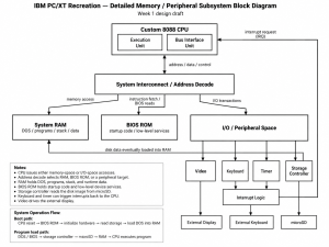
Diagram generated with Chat GPT
Josh’s Status Report (09/19)
This week, I focused mainly on researching the Intel 8088 specification and creating a block diagram for our custom CPU. I worked through how instruction fetching, decoding, operand reads, address generation, execution, and writeback connect, using an ADD instruction as a concrete example. I also studied how the bus interface unit shares memory access between instruction fetching and execution, along with how interrupts save processor state and redirect execution to a handler. While reviewing the diagram, I corrected inconsistencies in instruction decoding and address calculations and added missing data paths and control logic. This work helped me break the CPU into manageable components and better understand their interfaces before beginning RTL implementation. Next week, I plan to refine the control sequences and coordinate with Ben on the CPU bus interface so that our CPU and memory subsystem designs agree on how requests and responses are handled.
Govind’s Status Report (09/19)
This week, I primarily worked on the project proposal slideshow for our FPGA-based IBM PC/XT recreation. I also began expanding its high-level software design into the individual components shown in the diagram below. These include BIOS device support, DOS file and program services, and the shell, with .COM applications as the required target and .EXE support as a stretch goal.
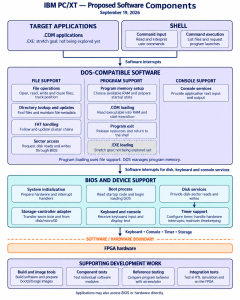
To guide implementation, I looked into Microsoft’s BIOS call reference, DOS system-call reference, and Ralf Brown’s Interrupt List. These document the software-interrupt interfaces, arguments, results, and error behavior that our software needs to support. My implementation plan is to work from basic BIOS and disk access upward to filesystem operations, program loading, and the shell. I plan to test each component using known inputs and expected outputs before integrating the next layer.
MartyPC will provide an emulated PC environment for developing our software and comparing program behavior. After verifying the setup, I plan to load a minimal custom ROM and inspect a known result in memory before adding BIOS functionality. Our FPGA-specific device interfaces will also require testing in RTL simulation and on the board.
I am behind on the scheduled MartyPC setup and sample code because this week’s effort went toward the proposal and design. Next week, I aim to complete the emulator setup, establish the custom-ROM test, and agree on the disk-access interface so I can begin BIOS and storage-adapter implementation.
Image credit: Created with GPT-6 Astra.