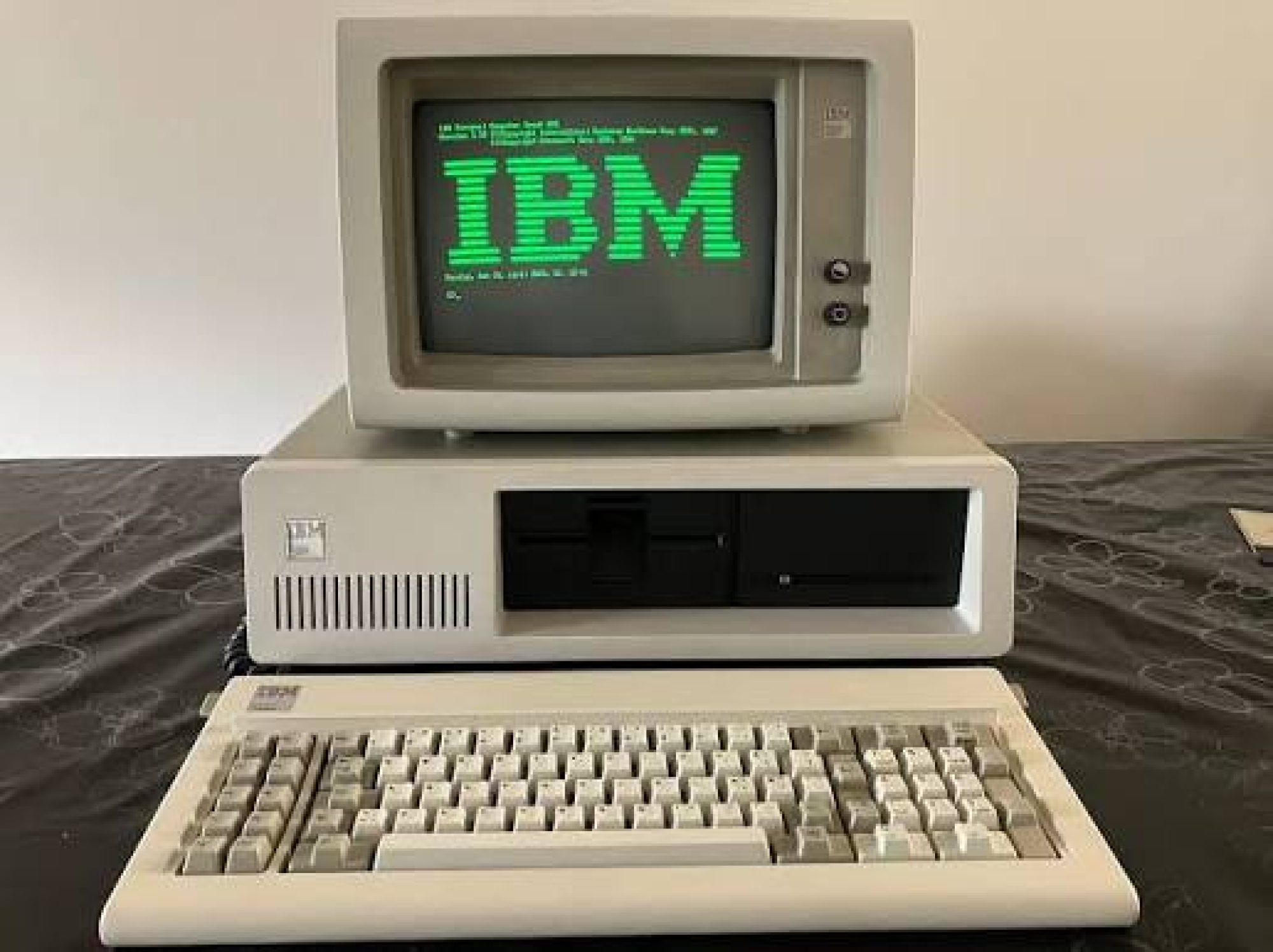
Team Status Report (10/10)

Josh added CPU memory accesses, stack operations, and CALL/RET. His tests covered memory delays, reset recovery, and original-8088 stack-pointer behavior, and caught all 16 deliberately introduced faults. Ben refined the design report’s memory/peripheral organization, interfaces, and testing plan. Govind extended EXE loading across the program arena and passed the expanded emulator regression.

Our main risk is CPU/firmware integration: remaining decoder, ALU, and interrupt work could delay BIOS execution. We will start with small diagnostic ROMs, then integrate BIOS services, while software development continues in the emulator. Ben reports his work is on schedule and will resume memory RTL integration next week. The next planned checkpoints are the October 19 FPGA diagnostic and October 26 BIOS/disk test; board-level verification remains pending. This week’s report revisions clarified interfaces without changing the overall architecture.

A was written by Ben Schlossman, B was written by Joshua Smith, and C was written by Govind Malasani.

Part A: Global factors
Our system is intended to help students and hobbyists beyond CMU study and modify a complete computer. Documented interfaces and emulator tests let others explore the design before obtaining an FPGA board. Hardware and tool access remain barriers, so our build instructions should state dependencies and avoid assuming access to a university lab. These access concerns are also identified in UNESCO’s educational-resource guidance.

Part B: Cultural factors
Our project serves the retrocomputing community’s interest in preserving older software and machine behavior. We check original-8088 behavior and document compatibility limits so users can assess which programs may work. We also write our own BIOS/DOS implementation and exclude copyrighted ROMs and game binaries from the repository. This approach reflects UNESCO’s digital-heritage principles, which recognize software’s cultural value alongside creators’ rights.

Part C: Environmental factors
The EPA identifies electronics reuse and recycling as ways to conserve resources and avoid air and water pollution. We plan to keep the FPGA board and peripherals reusable after the project and use existing compatible peripherals where possible. Emulator-based development lets us test software without additional hardware prototypes. System power consumption and lifecycle impacts remain unmeasured.

Govind’s Status Report (10/10)

This week I extended the MZ EXE loader beyond its original 64 KiB limit to use the existing 320 KiB program arena. I added reads and relocations across segment boundaries, checked code and stack addresses, and tested recovery from disk failures after partial loads. The full emulator regression passed all 22 guest profiles and 23 host tests. An earlier run timed out at 90 seconds; the unchanged code passed with an explicit 180-second process deadline. Evidence: https://github.com/JoshuaSmith1227/ibm-pcxt-fpga/pull/18.

The loader extension is complete. The November 2 shell/COM milestone still needs keyboard input and a minimal shell. Next week I will prioritize those features and their emulator tests while CPU and memory integration continues.

Josh’s Status Report 10/10

This week, I took the CPU from register-only programs to reading and writing memory, using a stack, and calling subroutines.

I gave the bus interface unit a second client, so data accesses share the bus with instruction fetch, with data going first when both request. I then added MOV loads and stores with BX-based addressing, a DS register and an address-generation unit. Each 16-bit access is two byte transfers on the 8088’s 8-bit bus, including words that cross a segment boundary or the top of memory.

Next I added the stack: an SS register, PUSH and POP, and near CALL and RET, which redirect instruction fetch like a taken jump. I checked PUSH SP and POP SP, where the 8088 differs from later x86 processors, against 10,000 recorded real-8088 cases each. A second write port for the stack pointer lets each instruction update everything on one clock edge.

Two repeatable demonstrations check registers, memory and every bus transaction under varied memory delays. The second runs two levels of subroutine calls and restores every register, including the stack pointer. Resetting the CPU in the middle of transfers exposed a bug where an interrupted load still wrote its register, which I fixed. The tests also caught all 16 deliberately broken versions of the design.

I also corrected our design report and added a CPU block diagram. Next are the full decoder, the remaining ALU operations, and interrupts, which the BIOS needs.

Ben’s Status Report (10/10)

This week, I focused mainly on working on our design report and making sure my portion of the memory and peripheral system was clearly documented. I helped refine the system architecture, memory organization, interfaces, and testing approach so that the report accurately reflects how my subsystem will connect with the CPU and software. I also continued reviewing the RAM, ROM, and address-decoding design to make sure it is consistent with the rest of the system. My progress is on schedule, and next week I plan to return to the RTL implementation and continue integrating the memory subsystem with the CPU interface.

Team’s Status Report (10/3)

Progress this week

This week, each part of the project moved further into implementation.

Josh connected the CPU’s instruction fetching and execution so it can run a short program from simulated memory. The program correctly moves and adds values, including when memory takes extra time to respond. He also added short jumps and tested that the CPU discards instructions from the old path when a jump changes where execution continues. He deliberately introduced bugs to check whether the tests caught them and documented the remaining test limitations.

Ben started implementing the memory system, including RAM, BIOS ROM, and the logic that directs each CPU request to the correct location. He also began tests for reading and writing RAM, reading ROM, and accessing the boundaries between memory regions. He and Josh are working through the timing rules for communication between the CPU and memory.

Govind’s software can now start in MartyPC using our own BIOS, bootloader, and C kernel. The kernel can open, read, and close files on a virtual disk, with tests for both successful reads and damaged data.

These are separate milestones. Our CPU has run small test programs in simulation, and our BIOS and kernel have run in MartyPC. We have not yet run the BIOS and kernel on our own CPU or demonstrated the complete system on the FPGA.

Main risks and backup plans

The largest near-term risk is connecting the CPU, memory, and software. Each has been tested separately, but differences in timing or expected behavior could cause failures when they are combined. Josh has written draft rules for CPU-to-memory communication and built checks for them. Ben is testing the memory modules against their expected behavior. The next step is to agree on those rules and connect the pieces using small programs before attempting a full boot. If integration fails, these smaller tests will help locate the problem.

Storage is another important risk. The selected DE10-Standard board’s microSD slot is connected to its ARM processor rather than directly to the FPGA. We therefore still need to settle how the FPGA will access storage. The emulator’s disk remains useful for continuing software development while this is resolved. A possible fallback for early integration is a small test image stored in FPGA memory, although that would not complete the final storage requirement.

The amount of work needed for DOS compatibility is also a risk. File reading works in the emulator, but keyboard input and loading programs are still unfinished. We plan to prioritize a small test program and the services it requires before expanding to more programs.

We also need to improve our code quality/practice. Although AI has been largely beneficial in terms of code development, we are falling behind on reviewing each others code which may be just as important. We hope to keep code review no more than a week behind implementation as well.

Design changes and their cost

The project documentation now identifies the Terasic DE10-Standard as our board. Its microSD wiring creates an additional storage-design decision that must be resolved before hardware integration.

For software testing, our BIOS currently uses the disk controller provided by MartyPC. This allows software work to continue, but the hardware-specific disk code will need to be adapted for our board. Keeping that code separate from the file-reading code limits how much software will need to change.

Schedule and next steps

We are continuing with the proposed schedule without a revision this week. Ben reports that the memory work is on schedule, and the CPU and software work have reached initial testing milestones. Storage access remains an open dependency that could affect later integration.

Next week, Josh plans to review the memory interface with Ben, define how devices will request the CPU’s attention, and add conditional jumps and more arithmetic and logic instructions. Ben plans to finish the initial memory modules and tests, connect them to the CPU interface, and begin device-address selection and storage work. Govind plans to continue keyboard input and program-loading work while reviewing the hardware-facing BIOS code with the team.

Evidence

– [Josh’s CPU progress and tests](https://course.ece.cmu.edu/~ece500/projects/f26-teama1/2026/10/04/joshs-status-report-10-3/)
– [Ben’s memory-system progress](https://course.ece.cmu.edu/~ece500/projects/f26-teama1/2026/10/03/bens-status-report-10-3/)
– [Software implementation and review guide](https://github.com/JoshuaSmith1227/ibm-pcxt-fpga/blob/govind/software-review/docs/software-review.md)

Govind’s Status Report (10/3)

Progress this week

I spent about 10 or more hours on the project this week, focusing on getting our BIOS and DOS software started and tested. I also spent four hours in class peer reviewing design review presentations, and additional time preparing for our presentation.

Our software can now start in MartyPC, an emulator that acts like an older IBM PC, using our own BIOS. The BIOS sets up the machine and reads our bootloader from a virtual disk. The bootloader then loads our kernel into memory and starts it. Earlier tests used an existing BIOS called GLaBIOS, but the current custom boot tests use our own BIOS.

I also worked on the C compiler setup and the code needed to start C programs without an existing operating system. This lets us write most of the kernel in C while using assembly for the low-level startup and hardware access.

The kernel can now find files by name and open, read, and close them. These operations are also available through a small set of DOS-compatible requests. Tests cover reading files spread across different parts of the disk, reaching the end of a file, opening missing files, and handling damaged disk data. This is still a test system: keyboard input, a command prompt, and loading existing DOS programs are not implemented yet.

Finally, I worked on making the implementation easier to understand and review. The documentation now explains how the emulator, BIOS, bootloader, and kernel connect, and the assembly comments explain what each instruction does.

Evidence:
– [Software explanation and review guide](https://github.com/JoshuaSmith1227/ibm-pcxt-fpga/blob/govind/software-review/docs/software-review.md)
– [Custom BIOS boot test results](https://github.com/JoshuaSmith1227/ibm-pcxt-fpga/blob/govind/software-review/docs/test-results/2026-10-03-custom-boot.md)
– [DOS file-service test results](https://github.com/JoshuaSmith1227/ibm-pcxt-fpga/blob/govind/software-review/docs/test-results/2026-10-03-dos-files.md)

Schedule

My progress is on track for the initial software setup and BIOS testing in our proposed schedule. Basic DOS file operations have also started. However, there is still substantial work before we can run existing programs, and all software testing so far has been in the emulator rather than on our FPGA.

Next week

I plan to check the display output directly, add basic keyboard input, and begin loading a small test program from disk and returning to the kernel when it finishes. I will also review the hardware interfaces with the team, especially how the BIOS will access storage on our board.

Josh’s Status Report (10/3)

This week, I took the CPU from a set of separate units to a working processor that fetches programs from memory and executes them, including branches and loops.

I started by defining the CPU side of the bus interface: single-byte transactions, where the CPU holds each request stable until memory signals completion after any number of wait cycles. I drafted these rules for review with Ben and built a simulated memory to stand in for his memory system.

On the CPU side, I implemented the bus interface unit, which captures instruction-fetch requests and returns each byte as memory completes it. In front of it I built a fetch controller with the 8088’s four-byte prefetch queue. It tracks its own fetch position and reserves queue space for requests already in flight, so the queue never overflows. I connected the fetch path to the execution unit in the CPU top level and added an architectural instruction pointer, kept separate from the fetch position, which runs ahead. The instruction pointer advances by each instruction’s length when it completes.

I then added control flow: the short unconditional jump and the conditional jumps JZ and JNZ, which test the zero flag. When a branch is taken, the execution unit sends the target address to the fetch controller, which redirects fetching there. It discards queued bytes and partially decoded instructions from the old path. Memory requests already on the bus can’t be cancelled, so it lets them finish and drops their bytes. A branch that isn’t taken simply continues to the next instruction.

With these pieces in place, the CPU runs a short counting loop loaded from an instruction-memory image at the 8088 reset address. It produces the correct final register values and instruction pointer, regardless of how slowly memory responds. One design observation is that the CPU is currently limited by instruction fetch rather than execution, since the bus delivers one byte every two cycles. That will matter when we tune timing.

I also updated our documentation for the team’s board choice, the Terasic DE10-Standard. Its microSD slot is wired to the ARM processor rather than the FPGA, which affects how we design storage access.

Ben’s Status Report (10/3)

This week, I focused mainly on starting the RTL implementation of the memory subsystem and turning the architecture I had planned over the previous weeks into actual modules. I worked on defining the CPU-to-memory interface with Josh and started implementing the basic RAM, BIOS ROM, and address-decoding logic that will sit between the 8088 and the rest of the system. I also worked through how memory reads and writes should be handled and how the decoder will determine whether a CPU request should go to RAM, ROM, or eventually one of the peripheral interfaces.  I also started setting up simple directed tests for RAM read/write behavior, ROM reads, and address-boundary cases so that each piece can be verified before integrating it with the CPU. This helped clarify some of the timing and interface details that still need to be agreed on between the CPU and memory sides. My progress is currently on schedule, and next week I plan to finish the initial memory modules and tests, connect them more closely to Josh’s CPU interface, and begin working on the next layer of the peripheral system, starting with the I/O decode and storage interface.

Team’s Status Report (09/26)

This week, we worked on the design presentation while continuing CPU and memory development. Govind focused on preparing and practicing the presentation and researching the compiler and emulator setup. Ben helped on the slides and refined the CPU/memory interface, RAM and BIOS ROM organization, address decoding, and their test plan. Josh implemented and tested the first connected portion of the CPU datapath.

Josh’s CPU can now execute a short testbench-fed program using MOV and ADD that produces AX = 14. The ALU passed more than 20,000 directed and reference-model checks. Deliberately introducing bugs also helped check the testbenches and exposed an execution-unit coverage gap to fix. The CPU does not yet fetch instructions from memory, so this is an initial datapath milestone rather than a complete processor.

Our biggest risk is integrating the CPU, memory, peripherals, and software on time, so we will agree on shared interfaces early and test small programs before attempting a full boot. If storage is delayed, we can continue testing with preloaded programs while prioritizing disk boot, the shell, and .COM execution over optional features.

MartyPC’s emulated hardware uses different interfaces from our FPGA system, so we will need to adapt the low-level drivers for each while keeping the higher-level software shared. This lets us test software in the emulator, but the FPGA interfaces will still need separate testing.

The software work is behind the original schedule because the MartyPC setup and BIOS/disk-adapter tests are not complete. During the week of September 28, Govind will prioritize the compiler-to-emulator workflow and initial disk-read tests. This puts the planned DOS file-service and loader/shell milestones at risk. We will reassess those dates next week; October 19 remains the target for BIOS boot and disk reads on the FPGA. Meanwhile, Josh will begin instruction fetch from simulated memory and expand instruction support, and Ben will begin implementing and testing RAM, ROM, and address decoding.

Part A: Public health, safety, and welfare

Our project addresses an educational need by giving students a computer system they can inspect and modify to understand how hardware and software interact. Its contribution to welfare is mainly through learning rather than a direct health application. We do not intend the prototype for safety-critical use. For physical safety, we plan to follow the FPGA board’s power and connection requirements, secure wiring, and document setup procedures. Clear diagnostics, reset instructions, and known limitations should also make the system less frustrating to use.

Part B: Social factors

Our intended users include students, educators, and computing enthusiasts with different levels of hardware and software experience. To make the project useful beyond our team, we plan to document the interfaces and provide small examples rather than assume everyone already understands the 8088 or DOS. The project also gives people with different interests a shared system to explore: someone working on software can follow a request down into the hardware, and someone studying the CPU can see how programs use it. Emulator examples could make the software easier to explore without immediate access to an FPGA board.

Part C: Economic factors

We want the project to provide a reusable platform for studying an early computer architecture without relying on original vintage hardware. However, we cannot claim it is the cheapest option without accounting for the FPGA board, peripherals, and development tools. We plan to reuse available equipment where practical and prioritize the core functionality before optional features. Development time is another cost: keeping the emulator and FPGA software largely shared should reduce duplicated work, while simulation should help us find problems before board-level debugging.

A was written by Ben, B was written by Govind, and C was written by Josh.

Govind’s Status Report (09/26)

This week, I spent most of my time working on the design presentation and practicing, since I will be presenting for our team. I focused on explaining how the CPU, memory, peripherals, and software fit together, along with our design choices and testing plan. I also worked on making the presentation clearer and keeping it within the time limit.

I followed up on our discussion about using Vitis HLS to generate RTL from C/C++ for testing. The main issue is that converting our BIOS or DOS into hardware would bypass the custom 8088 that is supposed to run it. HLS can test the hardware it generates, but that would not tell us whether our software runs correctly on Josh’s CPU or works with our memory and peripherals. For our project, maintaining that separate implementation would add work without answering the main integration questions.

I identified Open Watcom v2 as a candidate compiler for our software. Its 16-bit C/C++ compilers can generate 8088-compatible instructions using the -0 option. We would still need assembly startup code and a linker configuration for the BIOS ROM. My next step is to validate this with a small program before building more software around it.

I also looked into MartyPC for testing before our hardware is ready. My proposed setup would load our BIOS ROM and a disk image containing our boot code, DOS, and test programs. A build option could select between an emulator-compatible disk driver and a driver for Ben’s microSD interface. This would let me test software behavior, including loading files from an emulated disk, while developing the hardware separately. It would not verify our CPU or storage controller; those still need RTL and board-level tests. I have researched this setup but have not completed it yet.

My software work is behind the original schedule, which called for MartyPC setup during the week of September 14 and BIOS/disk-adapter tests during the week of September 21. To catch up, next week I will prioritize compiling a minimal 8088 program, loading our own ROM in MartyPC, and beginning disk-read tests. I will also work with Ben on the storage interface. These are prerequisites for the DOS file-service tests, so I will update that milestone based on what is working next week.