Team A0 – Weekly Status Report #7

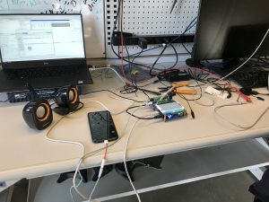
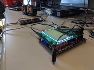
Since we were able to get audio passthrough working, we each of have been continuing on the other aspects of the project.

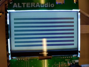
Nick P. has been working on researching how to implement FFT in verilog for the complicated effects that need the frequencies of a window of audio. Additionally he has been looking into the screen display protocol since it may be useful for real time hardware debugging.

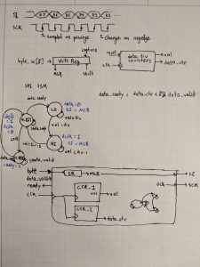
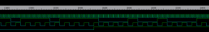
Nick S. has been working on getting the MIDI FSM decoder to work in hardware. This has been a combination of testing in simulation as well as testing in the board to make sure the essential key presses and velocity changes are working as intended.

Roshan has been working setting up the pipeline for all the audio effects. This includes the now working ADC/DAC modules, the synchronizing registers between the slower and faster clock domains, and the instantiation of the effect modules in the proper order.

Roshan Nair – Weekly Status Report #7

This week I have been working on implementing the micro architecture for the effects pipeline.

Since last week we were able to get audio pass through working by hooking up the adc data line to the dac data line within the fpga…this week we actually tested the shifting registers in verilog itself with the dac and adc interfaces. Initially we got extremely noisy audio. However I was able to fix the issue by changing the dac driver to be negedge instead of positive edge since the dac chip samples it on the positive edge.

Additionally instead of doing the native 24 bit audio we changed to 16 bit as defined by our spec and it seems to still have clean audio. Now I am working on setting up the synchronization registers for transferring the audio between clock domains (3.125 Mhz for dac/adc and 50 Mhz for effect processing).

Nick Paiva – Weekly Status Update #7

This week I’ve looked into the display driver and FFT more. I’ve tried to compile and run the FFT IP, but haven’t got it working. For the display driver, I’ve begun planning out its verilog implementation and looking at the controller datasheet. The display driver has a simple SPI interface with a few other pins that indicate if we are performing reads or writes and instructions or data. I’ve considered adding a FIFO to make the hardware design of the controller easier, but it doesn’t seem very necessary. The control FSM can be designed such that it only sends data when the hardware driver is ready. Here is my planning document for the display driver so far:

Nick Saizan – Weekly Update #7

This week my goal was to make some progress getting our main project code onto the fpga and integrating MIDI decoding into the synthesized code aswell. After wrangling with quartus and pin assignments files I was able to get our code synthesized along with MIDI decoding. Currently I am debugging some timing issues. It seems to read commands as expected sometimes and intermittently mishandles them during other times. I will need to think about various avenues of testing whether it be more testbench testing or potentially using signaltap. I will also analyze the code a bit more to see if I can identify the issues we’re having.

My current testing method involves displaying the pitch and pressure values. They are only displayed when the buttons are pressed.

Roshan Nair – Weekly Status Report #6

This week was primarily towards getting audio pass through working for the demo next week. Along with the general debugging that all of us had to do, I was in charge of setting up the basic verilog to drive the necessary clocks and pass the adc output to the dac.

To summarize: System Clock (25 Mhz), B Clock (3.125 Mhz), Word Clock (48.8 Khz)

Each of these were driven to the corresponding GPIO pins on the FPGA to properly control and configure the IC chips.

There were initial problems of the values not driving on the correct pins but this was due to the indexing bits in verilog being different than the actual physical pin.

Team A0 – Weekly Status Report #6

This week was mainly preparing for the first demo day. Out goal was to get just audio pass-through working This mean converting the audio signal to digital on the pcb running that through the fpga, and then converting back to analog on the pcb. Along with an audio source a set of speakers we got it working perfectly. The fpga doesn’t just act as a wire, it is also tasked with supplying the various clocks at different frequencies to the ADC and DAC ICs.

Demo Video

Nicholas Saizan – Weekly Status Update #6

This week all us us were very busy but we managed to work together to get audio passthrough working correctly. Initially when we setup the device it did not work on the first try. Nearly everything was working as expected except that the DAC was not outputting a signal. We did lots of testing of individual signals and components to isolate the issue. Eventually we learned it was a routing mistake on the pcb, which was easily resolved with a small jumper.

Roshan Nair – Weekly Status Report #5

This week has been primarily focused on efforts to get the mvp working. Therefore I have been continuing on with the adc and dac modules and verifying them. Additionally through discussion with my team members we came up with a plan for what the top level MVP module should look like. What we need initially for testing is just the ADC, DAC, and then a simple register to latch the audio values between them (no processing). This will be useful just to debug all the points of the system. From there we can move on with including panning and bit crushing in the pipeline for MVP effects.

This is an example of the ADC clock dividing by 8, the data lines getting latched in, and the word select line toggling after the 32 bits.