Roshan Nair – Weekly Status Report #6

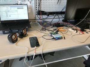
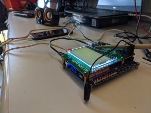
This week was primarily towards getting audio pass through working for the demo next week. Along with the general debugging that all of us had to do, I was in charge of setting up the basic verilog to drive the necessary clocks and pass the adc output to the dac.

To summarize: System Clock (25 Mhz), B Clock (3.125 Mhz), Word Clock (48.8 Khz)

Each of these were driven to the corresponding GPIO pins on the FPGA to properly control and configure the IC chips.

There were initial problems of the values not driving on the correct pins but this was due to the indexing bits in verilog being different than the actual physical pin.

Team A0 – Weekly Status Report #6

This week was mainly preparing for the first demo day. Out goal was to get just audio pass-through working This mean converting the audio signal to digital on the pcb running that through the fpga, and then converting back to analog on the pcb. Along with an audio source a set of speakers we got it working perfectly. The fpga doesn’t just act as a wire, it is also tasked with supplying the various clocks at different frequencies to the ADC and DAC ICs.

Demo Video

Nicholas Saizan – Weekly Status Update #6

This week all us us were very busy but we managed to work together to get audio passthrough working correctly. Initially when we setup the device it did not work on the first try. Nearly everything was working as expected except that the DAC was not outputting a signal. We did lots of testing of individual signals and components to isolate the issue. Eventually we learned it was a routing mistake on the pcb, which was easily resolved with a small jumper.