Callum’s Status Report for 3/17

This Week:

  • Found optimal distances for the wireless charger
  • Created a half-row model of the sensing array on a breadboard to test
  • Tested breadboard array with Android/Apple Phones and wireless earbuds
  • Sensitivity was weak for Androids – Added non-inverting amplifiers
  • Procured Opamps, Resistors, and Capacitors
  • Updated PCB model to reflect Opamp additions
  • Wrote sensor polling code and began device map code for the Arduino

Current Schedule:

Additions to circuit and supply chain problems still have our schedule somewhat behind. Still tons of slack in the schedule that we can use to catch up if we do not return to schedule by the end of the semester

Next Week:

  • Assemble PCBs (if they arrive)
  • Finish Arduino device map


Team Status Report for 3/16

Accomplishments

Whole Team – Long Ethics Assignment!

Anirud
– Enhanced PCB design, incorporating an op-amp and feedback resistors, crucial for improved sensor accuracy. Shifted all components to the top layer to eliminate interference with the wireless charger.

Luca
– Collaborated on revising the sensor array circuit diagram, integrating Op-Amps for better signal detection.
– Managed unexpected hardware issues: resolved a machining flaw in linear slides and dealt with a sudden laptop breakdown.

Callum
– Developed a half-row prototype of the sensing array, focusing on fine-tuning device sensitivity.
– Implemented non-inverting amplifiers to the array to clearly distinguish Android device signals from background noise.

Risk Management

– Supply Chain Delays: Actively monitoring supplier communications and exploring alternate component sources to minimize impact.
– Hardware Issues (Luca’s laptop, linear slide defect): Quickly addressing problems as they arise with practical solutions.

Design Modifications

– Op-Amps in Sensor Array: Added to increase the fidelity of device detection, especially for Android devices.
– PCB Layout Redesign: All components moved to the top layer to facilitate seamless integration with the wireless charging system.

Revised Schedule

In response to the recent challenges, we’ve adjusted our timeline to prioritize completing CAD work and assembling the full sensor array.

Project Highlights

– PCB Design: Anirud’s work on the PCB layout shows thoughtful problem-solving in response to integration challenges. https://drive.google.com/drive/folders/1UKzUN_nZ_kdPh8fONkxHx-t0Cf490zzb?usp=sharing
– Sensing Array Prototype: Callum’s prototype testing provided valuable insights for device compatibility and sensor adjustments.


Anirud’s Status Report for 3/16

What did you personally accomplish this week? Give files or photos that demonstrate your progress. Prove to the reader that you put sufficient effort into the project over the course of the week (12+ hours).

  1. Ethics Assignment: Completing the detailed readings and answering the questions took approximately 4-5 hours.
  2. Last week, I initiated the basic layout for the PCB without routing the traces. This week brought several additions to the board, such as an op-amp and feedback resistors, enhancing the reading resolution. Initially, I planned to position some components on the bottom layer of the PCB to minimize physical and electromagnetic interference with the sensors. However, to avoid interference with the movement of the wireless charger, I relocated all parts to the top layer. During our team meeting, we reviewed the board’s schematic and layout with Professor Fedder. Post-discussion with Luca about various mounting methods, I dimensioned the PCB for attachment under the acrylic/wood surface. We decided to laser-cut indents in the material to accommodate protruding components, allowing the PCB’s surface to be flush with the material. The PCB will be secured in place using liquid glue. Attached are a few images of the completed board.

Here is also a link to the drive folder with the images since their resolution is really bad here: https://drive.google.com/drive/folders/1UKzUN_nZ_kdPh8fONkxHx-t0Cf490zzb?usp=sharing

  1. Callum, Luca, and I dedicated time to perform distance characterization on the wireless charger we purchased. We tested its compatibility with various devices, including Android phones, iPhones, and wireless earbuds. Our approach involved placing layers of acrylic between the device and the charger to determine the maximum effective charging distance. Although results varied across devices, the charger’s performance exceeded our expectations and its advertised capabilities.


Is your progress on schedule or behind? If you are behind, what actions will be taken to catch up to the project schedule?

I believe my progress is on schedule. Although certain team tasks are behind schedule due to factors beyond our control, we’ve discussed these challenges as a team and recalibrated our approach. This ensures that we will be back on track by the end of next week.


What deliverables do you hope to complete in the next week?

  1. I aim to complete the sensor matrix polling code, in collaboration with Callum, by the end of next week.
  2. I need to acquire an Arduino Ammeter to measure the charge current. While this task appears straightforward, it’s crucial to verify that there are sufficient inputs available on the Arduino.
  3. I also plan to resolve how to manage the physical/mechanical aspects of the power cable for the charging coil, especially considering its movement on the gantry. It’s essential to ensure that the cables, both from this and other devices, do not become entangled as the gantry operates.
  4. Depending on when the ordered PCBs come in, I also want to complete the soldering of the through-hole components.


Luca’s Status Report for 3/16

What did you personally accomplish this week? Give files or photos that demonstrate your progress. Prove to the reader that you put sufficient effort into the project over the course of the week (12+ hours).

I worked with Callum on finalizing the circuit diagram for the sensor array. Thankfully we took another look at it, as we ended up needing Op-Amps, something we thought wouldn’t be necessary before. We also found that the hall effect sensors output a constant signal in the presence of a magnetic field (magnets) or phones in general. We previously believed that we’d only be able to detect a phone moving into range, not its position once stationary. While this will likely simplify later calculations and algorithms, it’s also a bit troubling: magnets produce a huge deflection while magnetless devices (many phones) create a very small deflection.
I also finally received the Amazon Prime 2-day shipping linear slides four weeks after placing my original order. While dimensioning them, I found an issue. One of the three cars is either incorrect or machined, manufactured so terribly that its threading is a fraction of a millimeter too small. Because of this, the M3 screws that are supposed to fit, don’t. While we could return it, and order a new one, we don’t believe that to be worth the wait. Thankfully, I was able to force in the screws with a bit of elbow grease. While this is certainly a passable solution, it’s also not a reliable one as the threads in the car or on the screw could break with repeated screwing and unscrewing.
I also had to “spend” time working on the ethics assignment, which took a few hours.
Lastly, my laptop died Thursday afternoon (the power supply to the main board suddenly stopped working). As such, I won’t be able to finalize the dimensions of the CAD and start printing until next week.

Is your progress on schedule or behind? If you are behind, what actions will be taken to catch up to the project schedule?

I personally believe I am behind as I wanted to have all the parts printing over spring break. However, all the delays are due to things out of my control:
– Orders not being placed when they were supposed to
– Orders arriving significantly later than they should, repeatedly
– Multiple incorrect components were delivered by Amazon
– Laptop spontaneously dying on me
I’m going to do my best to try and catch up next week, but I also have all my other classes to catch up with: re laptop.

What deliverables do you hope to complete in the next week?

The deliverables that were meant for this week, as the only one I accomplished was dimensioning the linear slides. To see them, look at last week’s blog.


Callum’s Status Report for 3/09

Last Week:
  • Created flow charts to visualize design clearly
  • Completed Design Review Report
This Week:
  • Created multiple schematic designs for the sensor PCBs so that Anirud and I could determine the best design with respect to prices on JLCPCB
  • Reviewed above schematics for errors
  • Received electronics components from shipping services
  • Edited design to include one extra row to ease workload when soldering PCBs. This change is reflected in the Desmos outline here
Current Schedule:

We’ve had some problems with shipping of materials which has held us back behind our current goals. This along with some of my own personal, external responsibilities has kept us behind schedule. That being said, most of this slack should be cleared in the next week as we order PCBs and can finally begin stage assembly.

Next Week:
  • Assist Anirud in finalizing PCB layout
  • Begin writing Arduino code for sensing and device mapping
  • Begin work on the final design for the user-interface and possibly begin wring code

Team Status Report for 3/09

Current Risks to the Project:
  • PCBs take longer than anticipated to ship
  • Motor speed is much more limited than expected
Design Changes:

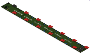
As stated in Callum’s report, we will be adding an additional row to the sensor matrix to ease workload when soldering the PCBs. This change was made as before, our grid had 9 rows of 7 sensors and 8 rows of 6 sensors; this layout made it difficult to design a repeatable PCB design such that we could avoid using one large (and expensive) board beneath the table surface.

A was written by Callum, B was written by Luca and C was written by Anirud.

Part A: Callum…

With the global adoption of smart devices for communication and entertainment in most fields, keeping devices charged is imperative to be connected to the rest of the world. By creating more convenient charging means, we can help people to become more productive, and stay connected to the online world which we find ourselves more and more reliant on each day. Chargin’ is a product that could help anyone and has the chance to make a positive impact on the world in total.

Part B: Luca…

This might not directly align with our project’s goals. It’s not publicly showcased, lacks essentiality, and wouldn’t significantly influence interpersonal interactions. Functioning solely as a convenience tool, its pricing, if an actual product, would likely be reasonable for widespread accessibility. Interaction with this device would typically occur within someone’s home. The cultural impact would be minimal, with perceptions possibly focusing on owners’ convenience rather than laziness. Guests, unless explicitly informed, would perceive it as a regular table. Ideally, they wouldn’t even realize their phone was charged upon picking it up.

Part C: Anirud…

In our “Chargin’” project, a significant focus is placed on environmental factors, with special attention to minimizing electrical power consumption, and its impact on both living organisms and natural resources. Our approach to environmental responsibility is multi-faceted:

1.    Sustainable Materials: We prioritize using sustainable, recyclable, or biodegradable materials in the construction of the table, thereby reducing waste and environmental impact.

2.    Energy Efficiency: The power management system in “Chargin’” is designed for optimal energy efficiency. This system smartly allocates power, activating only when a device is detected for charging and minimizing standby power consumption. Such efficiency not only conserves energy but also reduces the carbon footprint associated with power usage.

3.    Reduced Electrical Consumption: By implementing advanced technology to control and reduce electrical power usage, we actively decrease the operational costs and environmental impact of our product.

4.    Non-Toxic Materials: The selection of non-toxic materials in our design is aimed at safeguarding indoor air quality, ensuring a healthier environment for users.

5.    Lifecycle Consideration: The design includes plans for efficient recycling and disposal at the end of the product’s life, ensuring minimal environmental impact.

Luca’s Status Report for 3/09

What did you personally accomplish this week? Give files or photos that demonstrate your progress. Prove to the reader that you put sufficient effort into the project over the course of the week (12+ hours).

Last week, we spent a lot of time working on the design review document. Aside from writing within the document, I spent a lot of time rendering some very nice images of our design with solidworks. Those images are contained within this drive folder:
https://drive.google.com/drive/u/0/folders/1_GYA9Xxmdq5RgDXVgHwD4_M1uvIag3kI

Last week and this week, I’ve been dimensioning all the various parts that have arrived. While McMaster parts are very, very accurate to their included 3d models, the same can’t be said about Amazon. For example, the belt clamps are not two, but three times as thick as advertised. As a result, I had to fully re-design the lower middle of the stage just because of that one part. This has resulted in modifications being made to various other parts, which I won’t detail here.

Is your progress on schedule or behind? If you are behind, what actions will be taken to catch up to the project schedule?

I think as a whole we are on pace, but I am behind on my personal goal of having all mechanical components assembled and printing started by spring break. This is due to errors with ordering, both on our side, and from other parties. For example, the linear slides, arguably one of the most important parts of the entire mechanical assembly, weren’t ordered for some reason. There’s no record of an order being placed in the system for either rail, but in our team’s purchase tracker, both were marked as ordered. Something went wrong, but I worked with Tamal to rectify this and make sure all other orders had in fact been placed. Effectively, this resulted in waiting two weeks for parts to arrive that we never ordered. They should be here by Monday once ECE Deliveries has re-opened.

What deliverables do you hope to complete in the next week?

Barring even more issues with part deliveries, I should have the stage fully assembled, all parts dimensioned, and 3D prints started by end of next week. This will be heavily determined by when the linear slides and filament are actually delivered, but they should both be here next week.

Anirud’s Status Report for 3/09

What did you personally accomplish this week? Give files or photos that demonstrate your progress. Prove to the reader that you put sufficient effort into the project over the course of the week (12+ hours).

  • This week, I iterated with Callum on the schematic for the sensor array. Initially, we were going to make a PCB that covered half of the entire sensing area. We would then use 2 of them to cover the entire surface. However, we found out that JLCPCB charges a large fee for PCBs larger than a certain size. So, we reevaluated and reduced the PCB to the size of 2 hexagonally stacked sensor rows.
  • We also introduced decoupling capacitors between the VCC and GND for all of the Hall Sensors; on Professor Fedder’s advice.
  • We are also contemplating whether we need to introduce pull-up and pull-down resistors at VCC and GND respectively, to make sure that the sensors are reading the same voltage values, reducing the need for calibration.
  • I also completed the layout for the PCBs. We have two variants right now, one that has the capacitors as SMT components and the other one that has them as through-hole components. We are still trying to finish the cost analysis for the SMT vs. through-hole capacitors and are also trying to see if we can source them on campus, without having to purchase them.
  • The most crucial aspect of the layout was ensuring the alignment of the sensors and making sure that the distance between them was correct, according to the range characterization I had done earlier in the semester. I also had to consider the physical obstructions that would be there when we mount the PCB on the underside of the desk surface. I also positioned the pin headers to be out of the way and easy to access.
  • I am attaching the drive link for some of the layout images below. Note that I have not yet done the routing as I am waiting to do that till we have an internal design review for the schematic and make sure that the connections are 100% correct. The routing will take 45 minutes at most, so I am not worried about it. I will also be doing the routing for only one of the PCBs (either the one with the SMT or the through-hole capacitors)
  • https://drive.google.com/drive/folders/1UKzUN_nZ_kdPh8fONkxHx-t0Cf490zzb?usp=sharing


Is your progress on schedule or behind? If you are behind, what actions will be taken to catch up to the project schedule?

  • I think my progress as well as that of our team is on schedule!


What deliverables do you hope to complete in the next week?

  • Finalize the PCB layout and conduct a design review for it – with our entire team and a couple of professors, if possible, because we really can’t afford to mess this PCB up. I would also like to order the PCBs later next week.
  • Me and Callum will start working on the Arduino code for polling the sensors. We want to have it finished and reviewed by the time the PCBs arrive.
  • I also want to start integrating the charger and its peripheral circuitry. I need to figure out whether or not I need to use a Kilowatt to monitor peak current or if I can figure out a way to tap the PCB and get the charging current data.

Team Status Report for 2/24

What are the most significant risks that could jeopardize the success of the project? How are these risks being managed? What contingency plans are ready?
Currently, the main risks are if the stage design will be robust enough to support the tension in the timing belt, and if the sensor array will be accurate and reliable enough to detect devices. The former is being mitigated via front-loading of CAD and assembly to allow sufficient time down the line for debugging and likely slow reprinting of parts. A similar approach is being used for the sensor array. This week, we ran a small scale test to verify the practicality of using hall sensors. Fortunately, it appears this sensing approach is sufficient to detect devices, and next week full scale testing will hopefully begin. Like the CAD and mechanical assembly, we are allowing ourselves lots of time later in the semester to debug issues that will certainly arise.

Were any changes made to the existing design of the system (requirements, block diagram, system spec, etc)? Why was this change necessary, what costs does the change incur, and how will these costs be mitigated going forward?
Thus far, I believe there have been no major developments, other than sensor selection finalization. However, changes will likely begin to manifest in the coming weeks as actual implementation begins. The most likely being the layout of the sensor array as that is yet to be finalized, and minor adjustments to the CAD to accompany incorrectly listed Amazon parts.

Provide an updated schedule if changes have occurred.
Same schedule as last week, just moved one week forward.

This is also the place to put some photos of your progress or to brag about a component you got working.
While I’m unable to upload a video, the cad assembly is fully finished and works wonderfully. I can upload these renders of it, though. I expect there to be some actual photos by the next report.

Callum’s Status Report for 2/24

Personal Accomplishments:
  • Anirud determined the optimal range for hall effect sensors; I took the data and adjusted the Desmos diagram to represent this change. This brings our total number of sensors to 107.
  • Redesigned the circuit diagram to reflect the change in the number of hall effect sensors and the subsequent change in the number of 4051 switches.
  • Researched for an off-the-shelf Qi charger that gave a large range at a reasonable price ($20-$40).
  • Ordered 4051 ICs and wireless charger
Current Schedule:

We are mostly keeping on schedule, however, we were all very busy this week and were somewhat lazy in ordering parts which led to us slightly falling behind. That being said, we have plenty of schedule slack to make up for this missed time (inclusive of the fact that we plan to work some over Spring break).

I also believe that some more schedule adjustments need to be made to better reflect the total time needed to complete each task. We are much more aware of our requirements to complete a viable project and now understand what tasks are ahead of us.

Next Week:
  • Revamp Gantt chart
  • Build a small-scale sensor matrix and test
  • Finalize purchases and acquire all materials (that we currently plan to use)
  • Begin writing detection code