
This week was focused around working with Stefan and Archana to get the project ready for demo and making the slides for the final presentation. I worked with Stefan remotely to integrate the different systems and debug the hardware. I also made my share of the final presentation slides and met with the team to prepare for the presentation.
Harper’s Status Report for 4/24
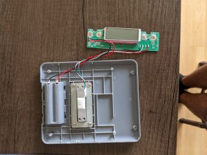
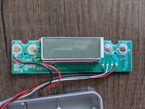
This week was focused around integration. Because I was able to make a trip to Pittsburgh, I brought with me the materials I had assembled to get the load cell to work with calibrated readings. I then worked with Stefan to integrate that into the LCD and enclosure.
Harper Status Report 4/10
This week was focused around preparing for the demo coming up on Wednesday. I started on making an arduino based load cell interface to show how the data would be collected once it is plugged into the STM32. I also ordered nrf24l01s to connect to the arduino so that we can start creating the pseudo bte connectivity for the app. Next week will be focused around making sure the disjointed demo is ready.
Harper’s Status Report for 4/3
This week was focused around the new load cell. After proving that it worked last week, I adapted the CAD model of the scale to include a model I made of the load cell. I had to guess the thread size based on the screw and a through hole ruler I have but we’ll be able to test it by 3D printing the threads when another load cell arrives in Pittsburgh.
Harper Status Report 3/27
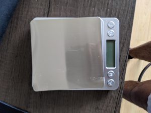
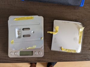
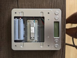
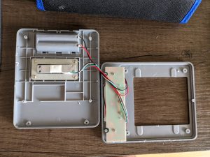
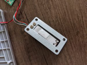
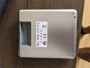
Due to concerns from the design report about the load cell, I ordered a development board for our load cell amplifier and an espresso scale that measures 500g with a resolution of .01g to remove the load cell and test if we can use it for our purposes. I disassembled the scale and found that the load cell inside uses the same Wheatstone bridge connection we use for the load cell amplifier so it should work electrically. Next weeks goal is testing if it will work with our amplifier and an Arduino. If so, the CAD will be modified to use this load cell with our PCB once it comes in. The disassembly process is documented below.
Harper’s Report for 3/20
This week’s focus was mainly the design report and finalizing design documents so that they could be included in that. This includes finalizing the power consumption analysis and double checking how everything connects within itself. Since I didn’t get to start looking into firmware this week like planned, that will be a priority next week.
Harper’s Report for 3/13
This week I focused on the verification documents for the PCB and the power consumption analysis for the system. The power consumption analysis was completed to the point where the verification documents needed. Further work on the verification documents will be done after some preliminary firmware is written so that we can test bring up software. Next week will be dedicated to firmware and getting estimates on battery life given the power consumption analysis.
Harper’s Status Report for 3/6
This week we finalized the PCB designs and submitted them for approval to the TA. Furthermore, I helped Stefan with the mechanical design of the shell so that we can plan for the physical spacing of the PCB in the overall design. Lastly, I started on the operational verification documents for the PCB so that we can begin on the functional use before the PCBs arrive.
Harper’s Status Report for 2/27
This week I worked on the PCB design and BoM with Stefan to make sure our circuit had all the components we needed and each IC would be kept within operating conditions. I then routed the PCB and sent it to PCBWay for approval. I also started on the Power Consumption Analysis. A preliminary look at it was well within reason at <5mA.
Harper’s Status Report for 2/20
During the first week I worked with the team to establish the beginning of our PCB bill of materials. I then took that and created the EAGLE footprints we need and put them together in the schematic. This required selecting which STM32 we’re to use as well as reading through the datasheet to verify which peripheral components we needed. I selected the STM32F423 for it’s compact blueprint and internal LDO. At this point we now have the JTAG connector, load cell/i2c, and voltage regulation laid out with the stm32. Once we have the interface buttons, LCD, and bluetooth setup we can do the layout and hopefully order the PCB next week.