This week, I resolved the shoot-through issues that the motor controller board was experiencing. This was mainly done by increasing the value of the H-bridge gate resistors until the MOSFET turn-on times were significantly longer than the turn-off times, generating dead-time in which neither MOSFET on a single side of an H-bridge is on. An acceptable shoot-through current spike specification was calculated by assuming that the shoot-through current was relatively constant for the duration of the spike (which was roughly 1 us in transient simulation), and relating the resultant flow of charge to a drop in the voltage of the H-bridge power supply output capacitors. By setting this maximal voltage drop to 0.03 V (so that the output capacitors retained 99% of the nominal output voltage after a shoot-through spike), I calculated that a maximum shoot-through current of 1.2 A for 1 us was satisfactory for the motor controller design. This maximum shoot-through current specification was found to correspond to a gate resistor value of 4152 Ohms in simulation. Setting the gate resistor to 4.22 kOhms (the nearest available value in Digikey) produced the following waveforms:
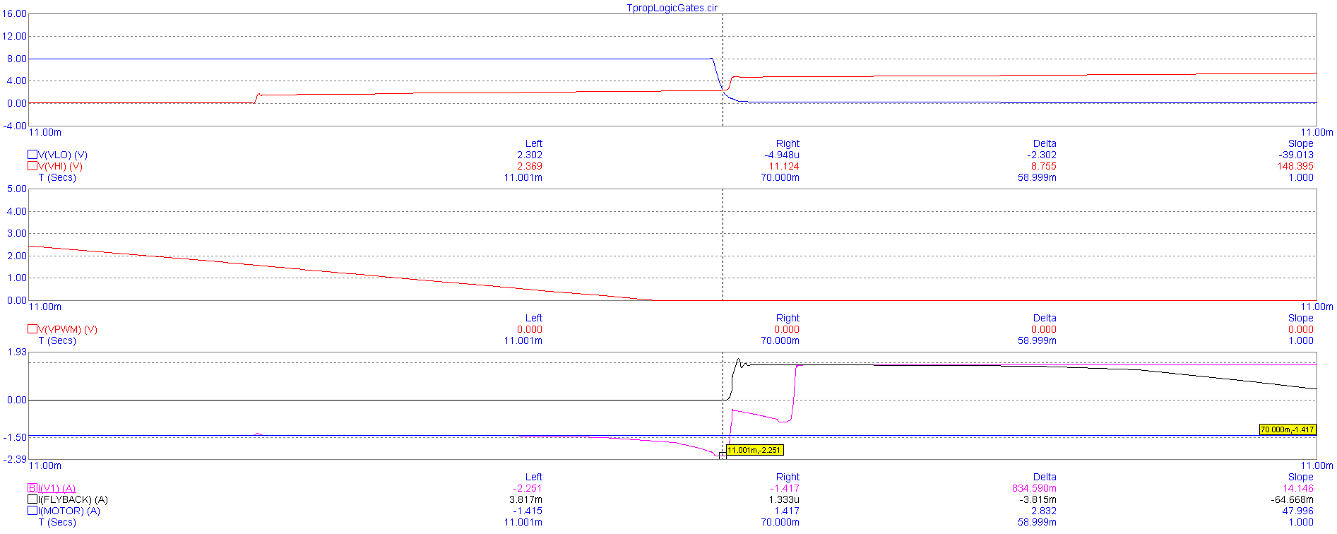
As can be seen from the pink waveform in the bottom-most plot, this value of gate resistor results in a shoot-through current spike of 2.251 A. From the waveforms of the hi-side and lo-side MOSFET gate voltages shown in the upper-most plot, we can see that the turn-on time (the red waveform) is much longer than the turn-off time (shown in the sharp edge of the blue waveform). Therefore, the circuit is operating properly for this value of gate-resistor.
Re-simulating for the circuit propagation delay, we find that the tplh of the PWM input is now 1.127 ms, while the tphl is 1.1 ms. Since this is much less than the period with which we plan to switch the motors, the gate resistors clearly do not overly impact circuit performance.
After making this refinement to the motor controller circuit, I generated a preliminary layout on PCB:
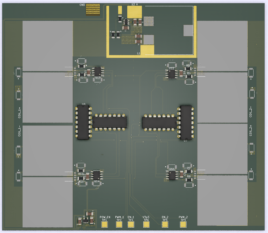
The 8V and 3V supply modules were pasted in from their respective layout files, while the remainder of the board was laid out in accordance with http://www.ti.com/lit/an/slva959a/slva959a.pdf. All that’s left is to place additional charge-storage capacitors at the power nodes. Here’s the updated schematic: schematic
I’m slightly behind schedule on this. I was supposed to complete the layout process earlier in the week, but ended up taking longer than expected. However, assuming that we follow the current schedule, all that’s left is to make the aforementioned revisions and perform a design review before ordering the board.
I’m uncertain as to what I should aim to complete next week. CMU’s recent move to remote instruction in light of the recent pandemic means that there will be substantial changes to the plan for capstone moving forward, and it’s unclear if there’ll still be a project component to this class.