Team Status Report
RISKS
We are in the interfacing phase of the project, which is said to be, and indeed, the most difficult part. The 2 biggest risk at hand is whether we can get the communication between our 3 parts(PL, SoC, Software) working, and whether we can make it work in time. We are on a very tight schedule. We must work as fast as possible for the following weeks before final demo.
DESIGN CHANGES
There were no significant changes made to the hardware design this week.
The seam-carving algorithm took a few more iterations after the demo on Monday. We noticed that the restricting the band-width of a seam produces a discontinuous sheet and therefore distorts the output video significantly. Therefore, we decided to try an algorithm where an average seam is computed per iteration, and the min-cut that most closely matches the average will serve as the radix point. All seams to the left and to the right of the radix would be re-computed sequentially, with its bandwidth being restricted as the three pixels surrounding its previous seam. This algorithm is still under development, but hopefully will work better than the previous.
UPDATED SCHEDULE
Maxwell and John have been working on the fabric-SoC interface this week, specifically the DRAM-SoC interface. This is slightly overdue, but we are making good progress on it and should have that working by Monday, which will make back about half of the time that we slipped by last week. Riki has completed the algorithm and is currently in the process of refining it to produce higher-quality outputs.
Maxwell Johnson
Personal work:
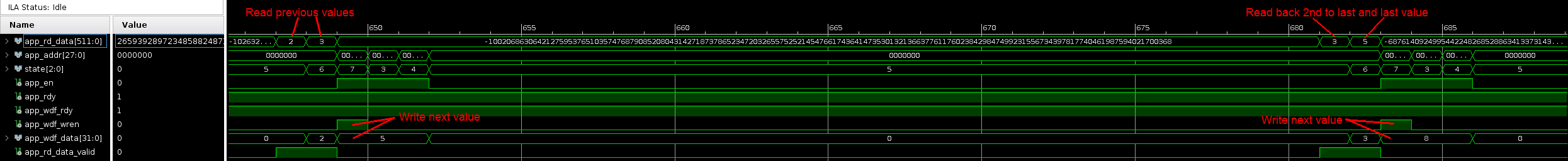
Shortly after last week’s update, I successfully interfaced to the DRAM on the board. Xilinx’s Vivado has the ability to create an example project using a custom IP (the DDR3 memory interface, in my case). This example is built to provide a test of the DRAM itself, and comes packed with useful debug functionality. However, I was unable to rework the traffic generator to be useful for our project. Ultimately, I did succeed in instantiating the IP in my own project with a simple FSM controlling memory access. My example computes Fibonacci numbers, storing them to memory and reading them back to compute the next value (Note: this is a terribly inefficient way to compute Fibonacci, but provides a good test of memory accesses). I learned how to use Vivado’s on-chip logic analyzer to generate debug waveforms. This section of the waveform shows an example calculation:
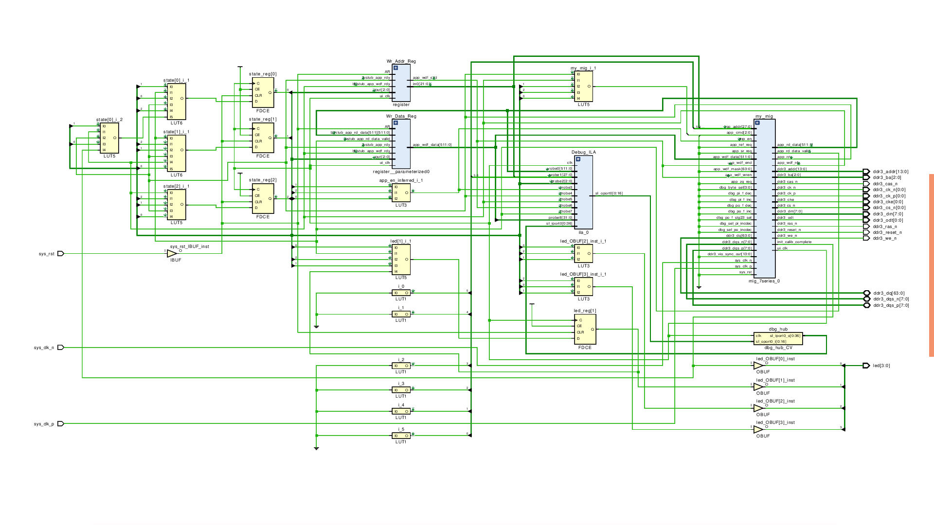
This is the datapath of this example, including the logic analyzer IP:
Progress:
My progress is slightly askew, as I cannot proceed with loading a video into the fabric until the interface with the SoC is complete. John and I have been working on this task, but we are still having difficulty working with the SoC. I’ve been investigating running an application bare metal and have a toolchain set up for that. I have a prototype of the energy-computing hardware from the design review, which is a great starting step on the development of the final design. This will be the starting point for my work next week.
Deliverables:
To avoid letting the SoC problems interfere with my schedule, I’ll be working on the energy-computing hardware this week while John figures out the SoC’s side of the DRAM interface. I’ll have a design complete by the end of next week, and hopefully we will also have the interface problems resolved.
John Zhang
Personal Work
This past week my main focus was on the communication between the SoC and the Programmable Logic.
Progress
My focus is on the SoC side of things. I was able to first achieve communication between my laptop and the Zynq board, and then boot a linux kernel on the board. I did a significant amount of research on how to achieve communication between the SoC and PL. The possible next steps are one of the following: get C scripts running on the linux kernel and thereby read from/write to memory; Use the IP block AXI to achieve communication.
Deliverables
Next week we’re looking to achieve communication between all of our 3 main components.
Riki Khorana
Personal Work
I’ve spent the entire week updating and refining the software application. Like I’ve written in the DESIGN CHANGES section, I worked on updating the algorithm to produce better quality videos.
Progress
I am still behind schedule-wise, as I do not have a set program to start running videos through. However I am certain that spending more time on the algorithm and the software itself is the main focus of this design project.
Deliverables
By demos tomorrow, I am required to complete an updated software application, as well as draw out the different subroutines I have in my algorithm for visual aid. The visual aid will serve to allow all team members to understand what can and may be accelerated using the FPGA.