
Bhuvan’s status report (Feb 23, 2019)
This week I spent time in the lab with Dhruva, trying to connect the photodiode transmitter-receiver circuit to the GPIO pins of the FPGA. We observed that the FPGA was able to receive and replicate a signal a the function generator but for some reason would receive and send only 0 when sent data from our transmitter receiver circuit.
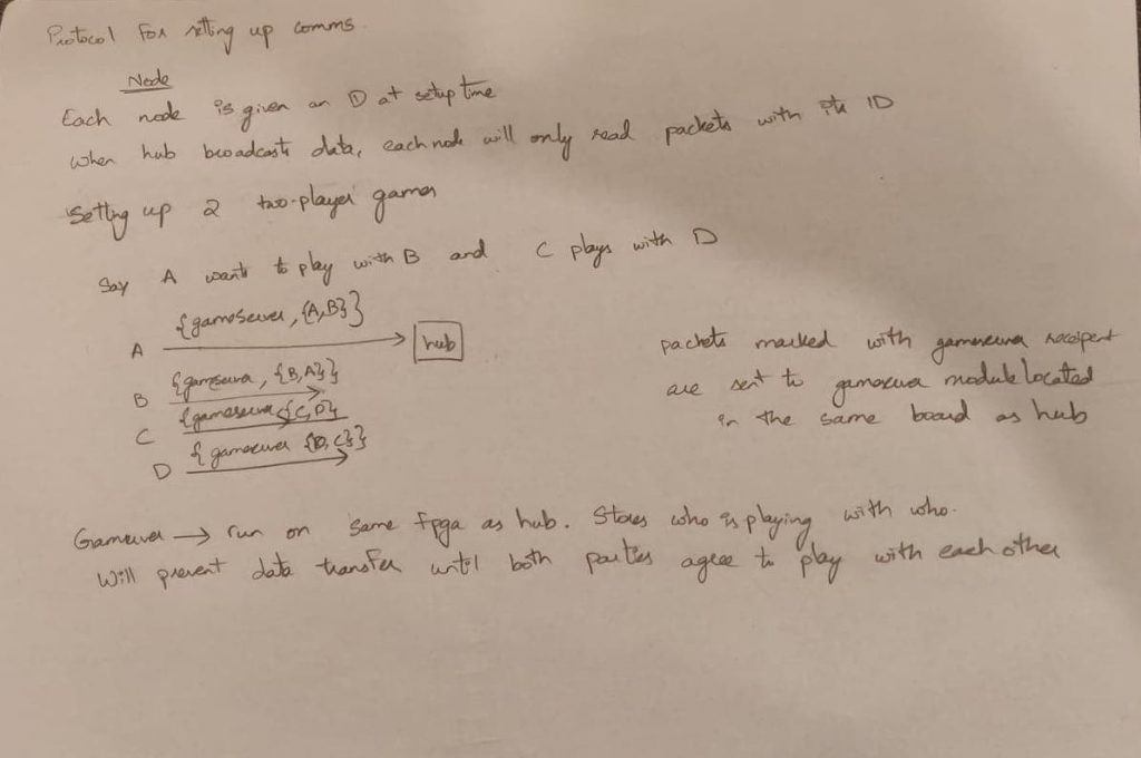
I also spent time designing the top level protocols for communication between the different nodes to send data about the players of the game and the game state.
The below picture shows a rough schematic for how players set up who they want to play against.
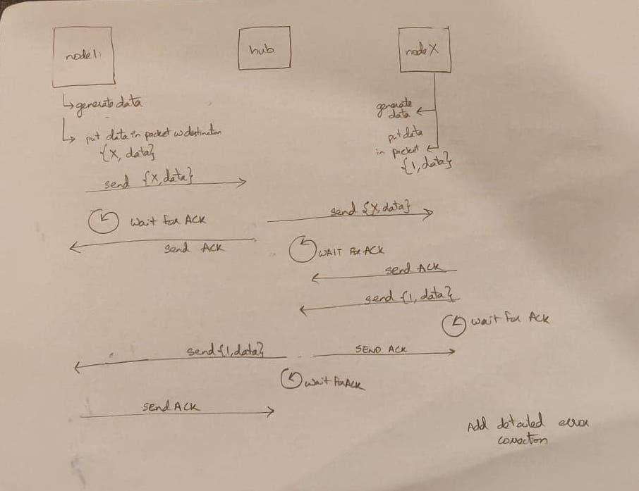
The below picture shows a rough schematic for how the nodes will send data to each other after the previous step.
I am in the process of drawing out a more detailed block diagram using draw.io and a more detailed UML diagram for the protocols using https://www.websequencediagrams.com, for use in the design presentation and report by Monday.
Dhruva’s Status Report (Feb 23, 2019)
This week, I worked on the circuit design and ran some preliminary experiments using the circuit we had built last week. This involved hooking up the circuit to the GPIO pins of the FPGA. The set up was as follows: a square wave input was connected in series to an IR LED and a resistor. The square wave from the function generator simulated the source of data which we expect in our final product to be coming from the source FPGA. On the receiver circuit, we had a trans-impedance amplifier circuit attached to an inverting op amp circuit whose output was connected to input pin 12 of the FPGA. The FPGA was programmed such that the input pin 12 was wired to pin 15 as well so we could observe the input to the FPGA through the oscilloscope as well the waveform viewer in SignalTap.
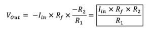
For a gain equation of a trans-impedance amplifier circuit, goes by
Vout = – Iin . Rf
where Iin is the current generated when the photodiode receives the pulses from the IR LED. From here the circuit is attached to a simple inverting op amp so the resulting output voltage of our receiver circuit is
Attached is the diagram of the circuit we constructed.
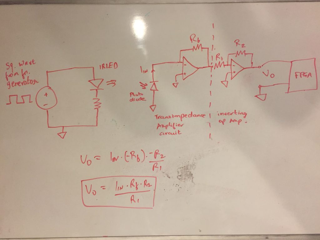
The FPGAs GPIO pin 12 was the input Vout input and pin 15 was debug output.
Now the task was to tweak values of Rf, R1 and R2 so that the FPGA is able to recognize the difference between a high and a low in the square wave. The goal was to try and ensure that the output at the GPIO pin 15 (the debug pin) would replicate the input square wave being sent from the function generator.
An ideal value of Rf was found to be in the order of 100kohms. Further exploration is yet to be done to determine whether the amplifier circuit is sending the data correctly to the FPGA, because on observing SignalTap, we were not able to receive any data in the FPGA.
I also researched protocols to handle the case when the transmitter and receiver are disconnected for a brief period of time (representing a network drop). For this project a network drop would mean a physical obstruction for a short time between the transmitter and receiver. Ideally we would like to have our network be able to recover the lost data in some way so I researched methods that do this.
In terms of the schedule, the design review is next week’s Monday so we put this part on pause and in the second half of the week as a group we focused on the high level design aspect of our entire project.
Raziq’s Status Report (Feb 23, 2019)
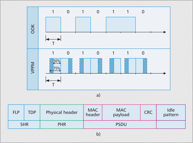
This week, I have narrowed down on the modulation and encoding schemes that we will use, given the hardware we have available and the targets we want to achieve. On-off keying (OOK) is a simple but effective modulation scheme that uses two different intensity levels to represent 1 and 0. Other modulation schemes like variable pulse position modulation (VPPM) and overlapping pulse position modulation (OPPM) could be used, but we do not have high energy efficiency requirements for our use case. Upstream modules address the concern about flicker mitigation (where “flicker” is defined as fluctuations in perceived brightness).
As suggested by the upcoming IEEE 802.15.7 standard, I plan to use Reed Solomon encoding (for example, RS(160,128)) as a means of forward error correction (FEC) because of its quoted suitability for indoor high-data-rate communications. 8B10B run length limited (RLL) coding is used to bound the length of runs of 1s or 0s to make clock and data recovery (CDR) easier and to reduce flicker. The 802.15.7 standard does not state that RLL can be used to achieve data rates up to 100 Mbps, but with recent improvements in VLC techniques (documented in many newer research papers) I expect being able to push the clock rate to support these encoding schemes.
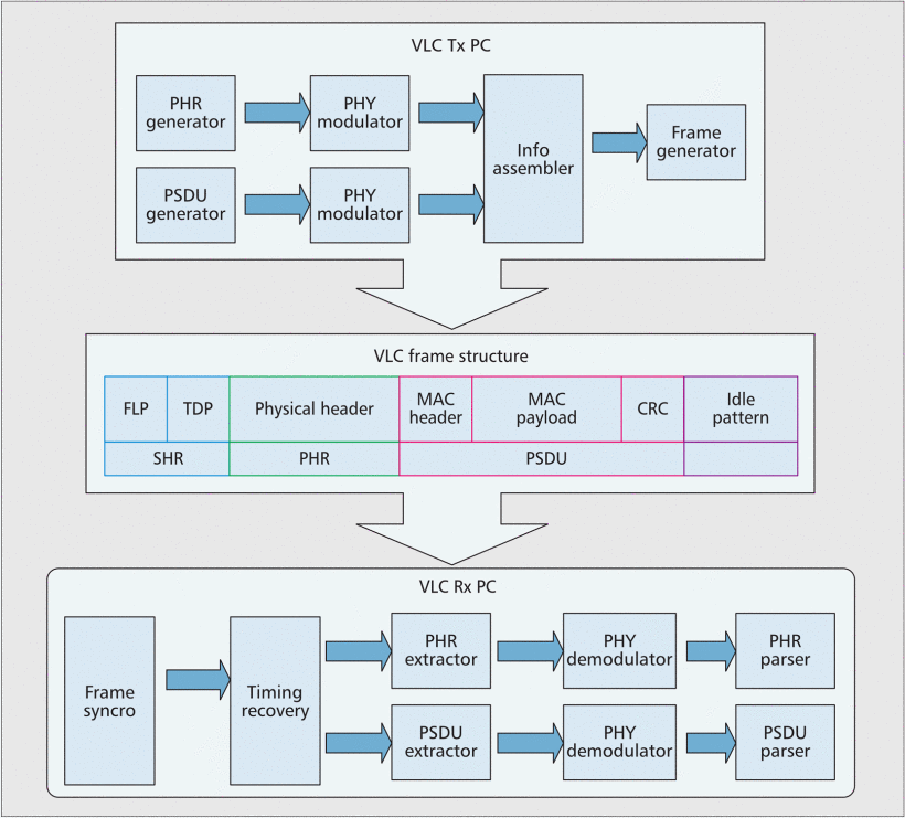
Below are diagrams of OOK modulation and of the datalink layer perspective of transmission/receipt from “Rapid prototyping of standard-compliant visible light communications system” (Gavrincea et al, 2014).
I personally did not make as much progress as I hoped due to some urgent deadlines. I had hoped I would have more rigorously defined our communications protocols and testing procedures. However, next week I expect to catch up on lost time due to fewer action items outside of capstone. After presenting during design review, I expect to finalize these design decisions in time for the report so that my teammates and I can advance to the implementation phase.
Upcoming work:
Fully design and document the finer details of the project over the course of the weekend
Perform research on games that can be portable/playable on an FPGA and begin work on tweaking it to work with our design
Finalize the circuit such that the data is being transmitted in an accurately.
Research the Verilog circuit FSM for error correction, correctness checks and off-by-one errors so that data is not dropped during transmission.
Research protocols to handle the case when the transmitter and receiver are disconnected for a brief period of time.
Build the receiver so that a square waveform from the function generator is seen in the FPGA.
Team Status Report
As a team, we are working on getting the slides ready for the design presentation. We are drawing detailed schematics, block diagrams and UML diagrams to describe the protocols and working of our project.
We met with Professor Tamal on Wednesday and received feedback on what to include in our presentation and are working towards that. We are currently on track with our proposed timeline. It appears next week is going to be especially busy due to the design review and a large volume of research and implementation work.