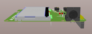
I have not gotten as much done this week as I would have liked due to job search stuff. That being said, I worked on a few different things this week. I spent some time figuring out how the ADC/DAC I2S drivers will work, as well as figuring out what manufacturing parameters to order the PCB with. If we use PCBWay and solder the components by hand, the PCB will be quite cheap (~$30). The components that go on it will be another $50. Here is my planning so far for the ADC driver:
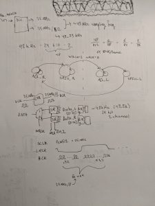
The verilog implementation of this driver should be pretty simple.
Additionally, I’ve looked more into how to implement digital frequency filtering and pitch shifting in the Fourier domain. I think that spectral leakage may be an issue with this technique, but that we can mitigate it with some clever processing.