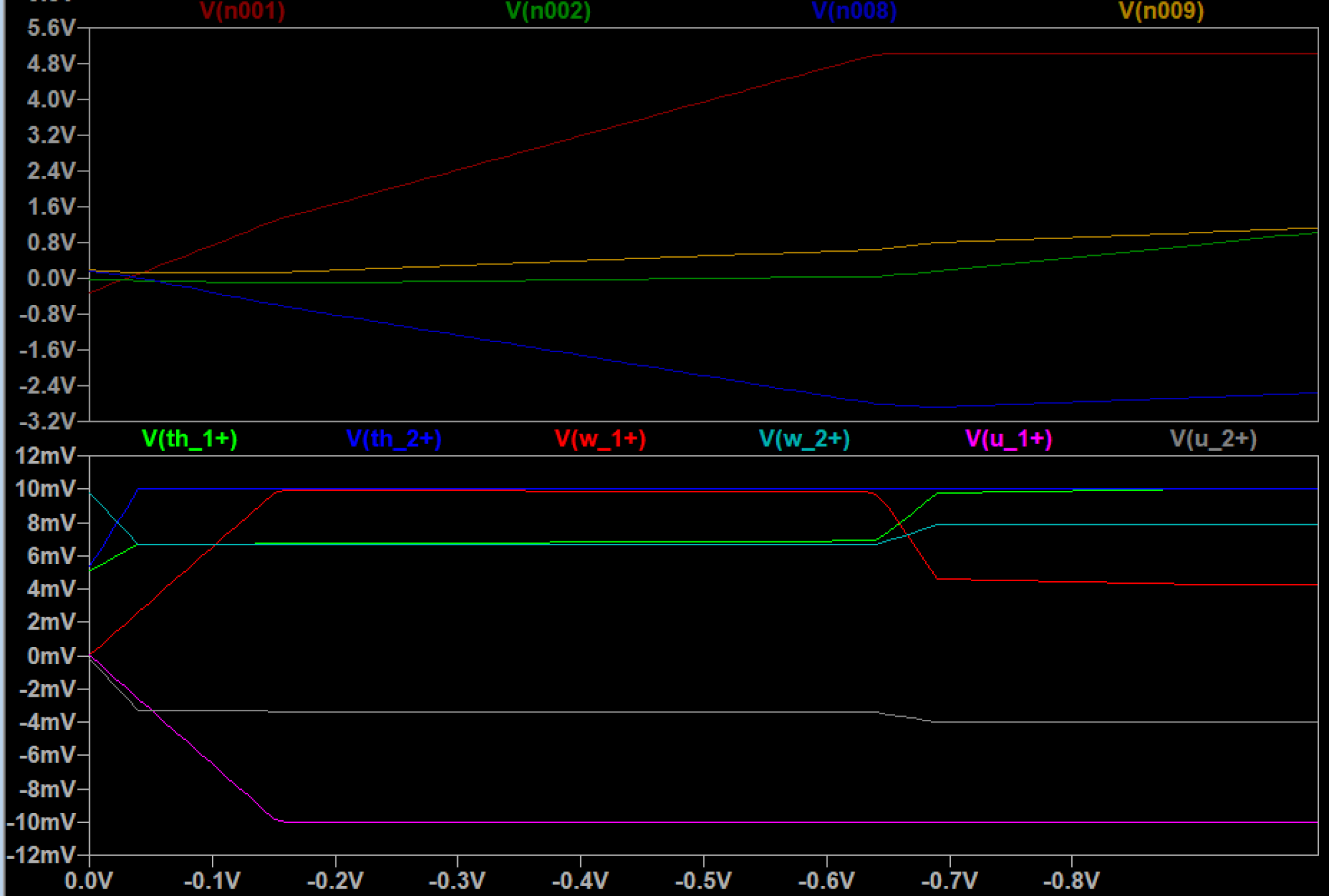
Overall progress:
On the software side, what is left is finishing the software-hardware interface. On the hardware side, we need to finish the layout for the PCB and send it out for shipping.
Significant risks and risk management:
Risk: Shipping the PCB on time
Description: Figuring out the routing/layout of the PCB is taking longer than expected. This is partially due to the fact that we need to verify the correctness of different parts of the board.
Severity: If we are unable to finish the layout before next Tuesday, we run the risk of not being able to ship the PCB in time.
Resolution: We are currently putting in as much time as possible to finish the layout.
Risk: While the circuit seems to work properly, we still need to properly identify what kinds of issues arise in the physically circuit
Description: We were able to predict much of the behavior of the “real world” circuit by using the components specified in the BOM. However, the actual behavior of the circuit will obviously be different
Severity: If the inaccuracies of the physical pcb are not properly accounted for, the circuit can have a variety of errors, including non-convergence and solutions with high error.
Resolution: We are currently modeling the behavior of some of these real-world effects as electrical components. For example, we have capacitors on the op amps that do not exist in the theoretical formulation, but exist in the real world analogue due to the parasitic capacitances. However, there are many more places where these issues can occur. The largest source of error compared to the circuit is the transition from resistors to linpots.
Changes to the existing design:
There are currently no significant changes to the existing design.
Changes to the project schedule:
We are trying to put as much time as we can to finish the PCB.
